Back contact structure of cadmium telluride thin-film solar cell, solar cell, cell assembly, and preparation method

A thin-film solar cell, back-contact structure technology, applied in electrical components, circuits, photovoltaic power generation, etc., can solve problems such as high resistivity and unsatisfactory batteries, and achieve the effect of reducing manufacturing costs

Inactive Publication Date: 2014-04-30
HENGJI WEIYE INTPROP MANAGEMENT CONSULTANTS BEIJING
View PDF3 Cites 4 Cited by
  • Summary
  • Abstract
  • Description
  • Claims
  • Application Information

AI Technical Summary

Problems solved by technology

MoOx is an oxide semiconductor material with a relatively high work function, and it is a relatively excellent back contact material. At present, good results have...

Method used


Image

  • Back contact structure of cadmium telluride thin-film solar cell, solar cell, cell assembly, and preparation method
  • Back contact structure of cadmium telluride thin-film solar cell, solar cell, cell assembly, and preparation method
  • Back contact structure of cadmium telluride thin-film solar cell, solar cell, cell assembly, and preparation method

Examples


Embodiment 1

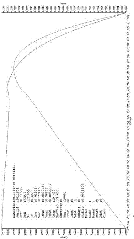
[0024] The back contact structure of the present invention is 0.5Mo 2 N-0.5MoO 2 battery.

[0025] Preparation method and conditions: 120nm thickness prepared by magnetron sputtering, Ar / O2 / N2=0.95 / 0.02 / 0.03, sputtering pressure 2.5Pa, substrate temperature 150 degrees, sputtering power 200W.

[0026] After sputtering 0.5Mo 2 N-0.5MoO 2 Post-layer annealing, the annealing temperature is 200 degrees, and the annealing time is 40 minutes.

[0027] according to figure 1 As shown, the J-V test results are as follows, the efficiency can reach 11.556%, the open circuit voltage is 775mV, the fill factor is 0.66, and the short circuit current is 22.48mA / cm 2 .

Embodiment 2

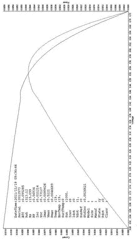
[0034] The back contact junction is Cu / 0.5Mo 2 N-0.5MoO 2 battery.

[0035] Preparation conditions:

[0036] Cu layer: 5nm prepared by magnetron sputtering, sputtering pressure: 2.4Pa, substrate temperature: room temperature, power: 100w (round target with a diameter of 110mm).

[0037] 0.5Mo 2 N-0.5MoO 2 Layer: 120nm thick prepared by magnetron sputtering, Ar / O2 / N2=0.95 / 0.02 / 0.03, sputtering pressure is 2.5Pa, substrate temperature is 150 degrees, sputtering power is 200W.

[0038] After sputtering 0.5Mo 2 N-0.5MoO 2 Post-layer annealing, the annealing temperature is 200 degrees, and the annealing time is 40 minutes.

[0039] according to image 3 As shown, the J-V test results are as follows, the efficiency can reach 13.15%, the open circuit voltage is 786mV, the fill factor is 0.67, and the short circuit current is 23.97mA / cm 2 .

[0040] Comparative example:

[0041] The back contact structure is Cu / Mo 2 N battery.

[0042] Preparation conditions:

[0043] C...

Embodiment 3

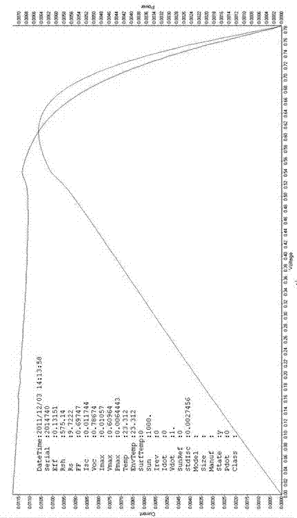
[0049] A cell with a back contact junction of 0.7MoN-0.3MoO3.

[0050] Preparation method and conditions: 120nm thickness prepared by magnetron sputtering, Ar / O2 / N2=0.94 / 0.04 / 0.02, sputtering pressure 2.5Pa, substrate temperature 150 degrees, sputtering power 200W.

[0051] After sputtering 0.7MoN-0.3MoO 3 After layer annealing, the annealing temperature is 220 degrees

[0052] according to Figure 5 As shown, the J-V test results are as follows, the efficiency can reach 10.834%, the open circuit voltage is 789mV, the fill factor is 0.615, and the short circuit current is 22.3mA / cm 2 .


PUM

PropertyMeasurementUnit
Thicknessaaaaaaaaaa
Thicknessaaaaaaaaaa
Short circuit currentaaaaaaaaaa

Abstract

The invention, which belongs to the new energy material and device field, especially relates to a back contact structure of a cadmium telluride thin-film solar cell, a solar cell, a cell assembly, and a preparation method. According to the technical scheme, the back contact structure that is arranged between a cadmium telluride absorption layer and a back electrode layer is a mixture layer with molybdenum nitride and molybdenum oxide; and the structure is expressed by (1-A) molybdenum nitride-A molybdenum nitride, wherein the A is larger than 0 and is less than 1. The work function of MoOy is high and the conductivity of MoNx is good; and thus, on the basis of combination of the MoOy material and the MoNx material, the back contact material can have advantages of the two kinds of materials.

Description

technical field [0001] The invention belongs to the field of new energy materials and devices, and in particular relates to a back contact structure of a cadmium telluride thin film solar cell, a solar cell, a cell component and a preparation method. Background technique [0002] Cadmium telluride (CdTe) thin film solar cell is a compound semiconductor thin film solar cell with CdTe as the absorbing layer. Because of its high efficiency and low cost, it has attracted the attention of many research institutes and companies. At present, the highest conversion efficiency of this cell is 17.3%, large-area modules (1.2×0.6m 2 ) with a conversion efficiency of 13.4%. [0003] The structure of CdTe thin film solar cell is: glass / transparent conductive film / window layer / absorber layer / back contact layer / back electrode layer. The absorption layer CdTe is p-type, and its electron affinity is ~4.3eV, and the band gap is ~1.5eV. It is difficult to find a metal material with a higher w...

Claims


Application Information

Patent Timeline
IPC IPC(8): H01L31/0224H01L31/18
CPCH01L31/022441Y02E10/50Y02P70/50
Inventor 蒋猛张征宇
Owner HENGJI WEIYE INTPROP MANAGEMENT CONSULTANTS BEIJING
Why Eureka
Try Eureka