Carbon nano-tube array with uniform tube diameter and growing method thereof
A carbon nanotube array and tube diameter technology, applied in the field of nanomaterials, can solve problems such as uneven distribution of tube diameters, and achieve the effects of reducing the possibility, the method is simple and easy, and the shape is improved
- Summary
- Abstract
- Description
- Claims
- Application Information
AI Technical Summary
Problems solved by technology
Method used
Image
Examples
Embodiment 1
[0034] An alumina buffer layer with a thickness of 20 nm and an Fe catalyst layer with a thickness of 8 nm were sequentially deposited on a 20 μm tantalum foil by vacuum electron beam evaporation. The composite substrate was put into a CVD tube furnace, and the temperature was raised to 650° C. at a rate of 10° C. / min in an argon atmosphere; then hydrogen gas was introduced, and the catalyst was reduced for 10 minutes at a pressure of 5 kPa. Then the temperature was raised to 700° C., and a mixed gas composed of argon, hydrogen, and acetylene was introduced, with flow rates of 140 sccm, 60 sccm, and 10 sccm respectively, and a total pressure of 30 kPa, and grown for 40 minutes. Finally, the heating was turned off, and the temperature was lowered to 550° C. at a rate of 10° C. / min under a low pressure of 7 kPa in an argon atmosphere, and then naturally cooled to room temperature.
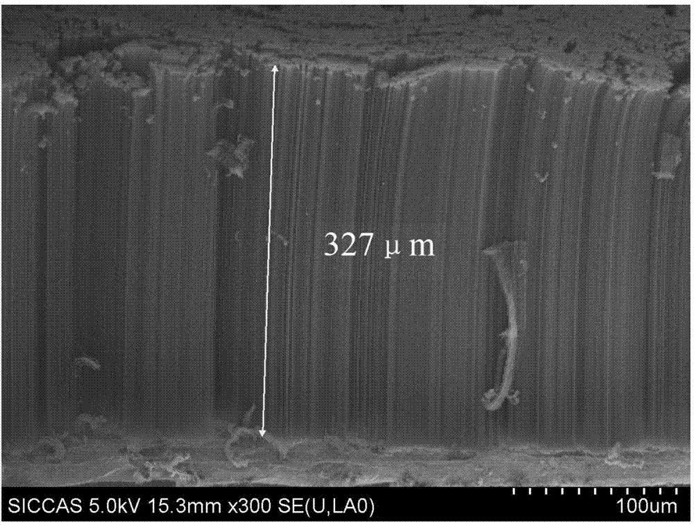
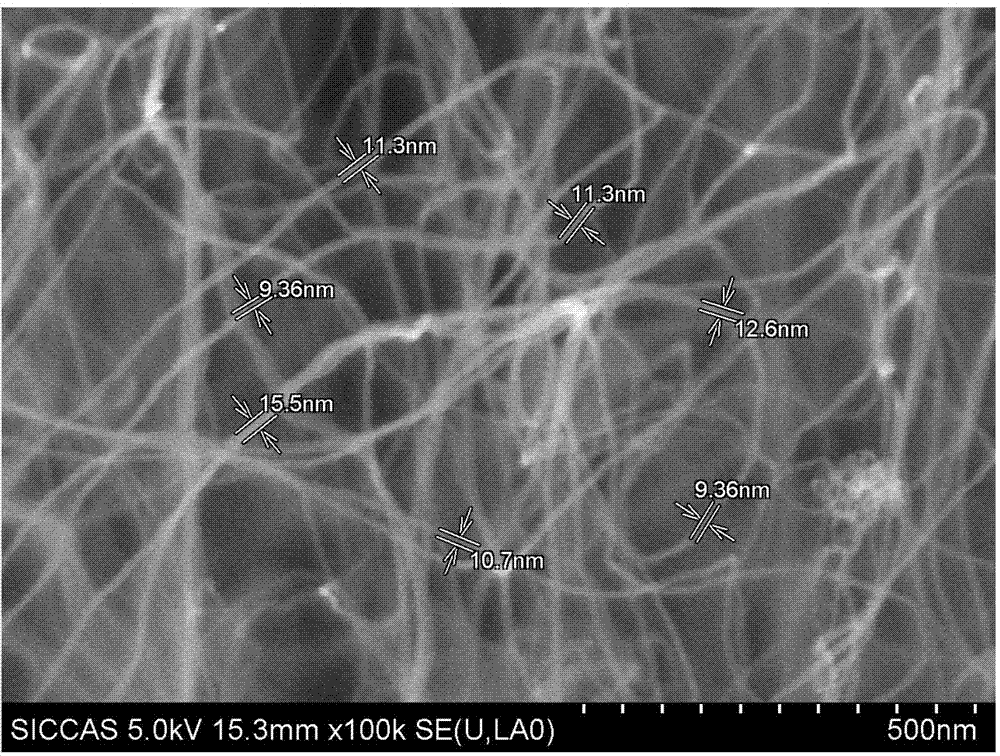
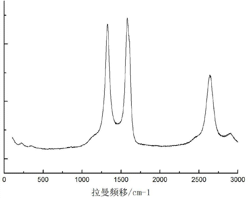
[0035] figure 1 It is a scanning electron microscope photo taken at an angle of 45° on the sampl...
Embodiment 2
[0037] The growth process is the same as that in Example 1, except that the catalyst reduction treatment is carried out at a low pressure of 10 kPa.
[0038] Such as Figure 5As shown, the height of the obtained carbon nanotube array is 221nm, closely arranged along the vertical direction of the substrate, and there is no amorphous carbon particle. Raman spectrum showed I(D) / I(G)=0.96. Such as Figure 6 It can be seen that the diameters of carbon nanotubes are distributed between 10 and 15 nm, and the standard deviation of the diameters is 1.39 nm, which is relatively uniform. Transmission electron micrographs show that there are obvious cavities, and the tube wall is composed of 5-8 carbon layers.
Embodiment 3
[0040] The growth process is the same as that in Example 1, except that the catalyst reduction treatment is carried out at a low pressure of 20 kPa.
[0041] The height of the obtained carbon nanotube array is 160 μm, and the carbon nanotube array is closely arranged along the vertical direction of the substrate, and there is no amorphous carbon particle. Raman spectrum analysis shows: I(D) / I(G)=0.98. The diameter of the carbon nanotube is 10-15nm, the standard deviation of the tube diameter is 2.67nm, and the tube wall is composed of 5-10 carbon layers.
PUM
| Property | Measurement | Unit |
|---|---|---|
| height | aaaaa | aaaaa |
| diameter | aaaaa | aaaaa |
| diameter | aaaaa | aaaaa |
Abstract
Description
Claims
Application Information


