Preparation method of active region failure analysis sample of semiconductor device

A technology for failure analysis samples and semiconductors, which is applied in the manufacture of semiconductor/solid-state devices, the preparation of test samples, and the testing of single semiconductor devices. Effect of suppressing ionization and avoiding damage

Active Publication Date: 2014-05-07
SEMICON MFG INT (SHANGHAI) CORP
View PDF11 Cites 7 Cited by
  • Summary
  • Abstract
  • Description
  • Claims
  • Application Information

AI Technical Summary

Problems solved by technology

[0005] The invention provides a method for preparing a sample for failure analysis of the active area of ​​a semiconductor device to solve the problem that the active area is easily damaged by removing the oxide layer and the polysilicon layer when making the sample for failure analysis of the semiconductor device with a deep trench structure

Method used


Image

  • Preparation method of active region failure analysis sample of semiconductor device
  • Preparation method of active region failure analysis sample of semiconductor device
  • Preparation method of active region failure analysis sample of semiconductor device

Examples


Embodiment Construction

[0023] In order to make the purpose, technical solution and advantages of the present invention more clear, the present invention will be further described in detail below with reference to the accompanying drawings and examples.

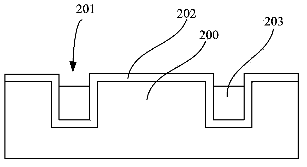
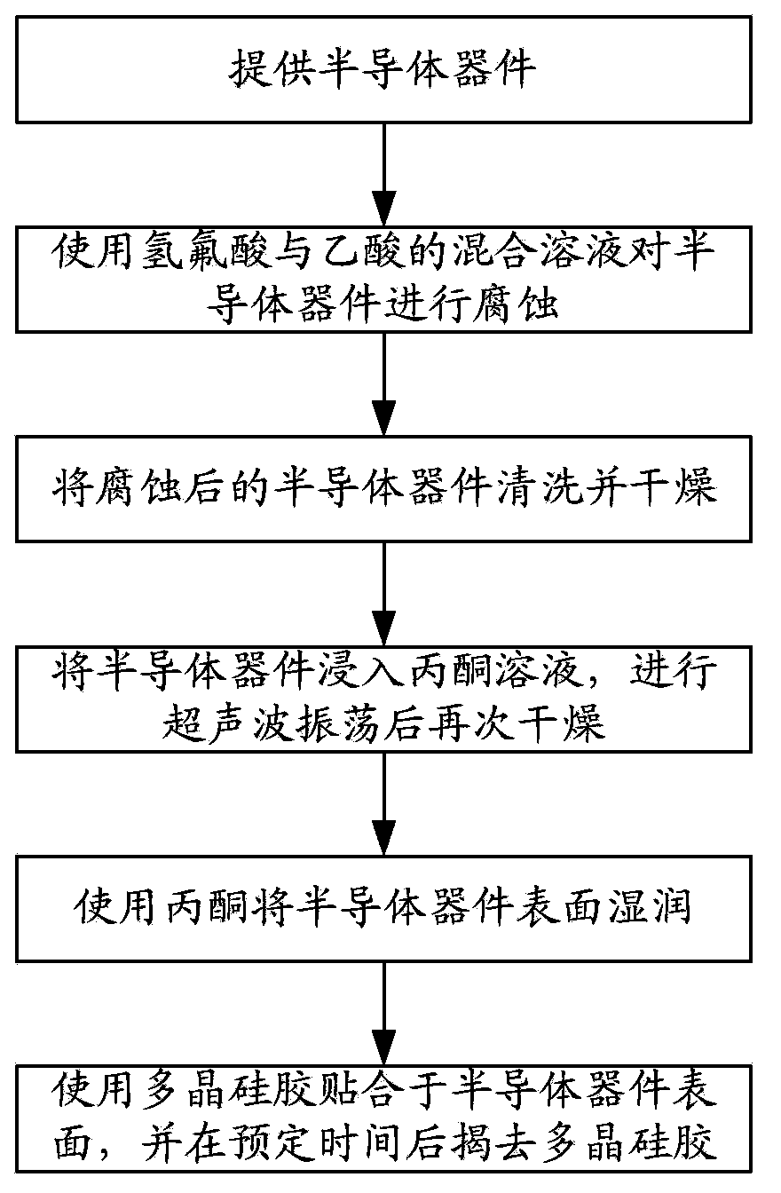
[0024] like figure 2 As shown in the flow chart, the present invention provides a method for preparing a semiconductor device active region failure analysis sample, including:

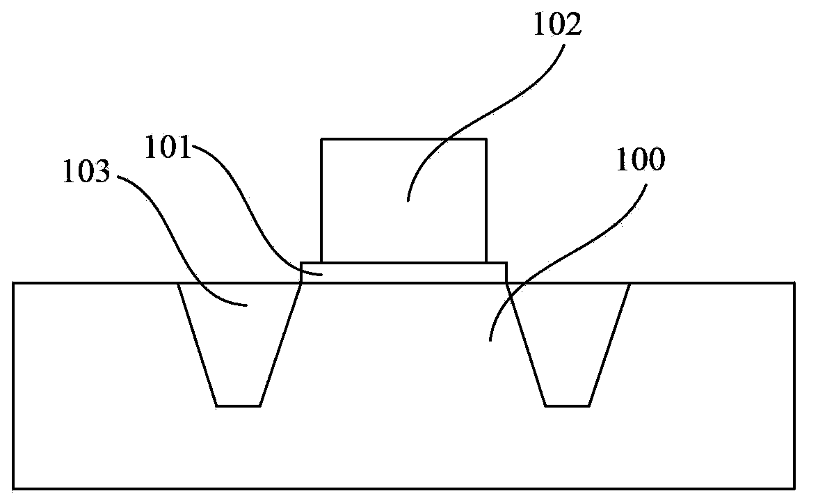
[0025] A semiconductor device is provided, the semiconductor device comprising an active region, a deep trench formed in the active region, an oxide layer covering the surface of the active region and the deep trench, and a polysilicon layer filled in the deep trench ; Wherein, the surface of the polysilicon layer is lower than the surface of the active region;

[0026] Corroding the semiconductor device with a mixed solution of hydrofluoric acid and acetic acid;

[0027] Cleaning and drying the corroded semiconductor device;

[0028] Immerse the dried semiconductor devi...


PUM


Abstract

The invention provides a preparation method of an active region failure analysis sample of a semiconductor device. A mixed solution of hydrofluoric acid and acetic acid replaces hydrofluoric acid simply used in the prior art to remove an oxidation layer; compared with strong corrosion of hydrofluoric acid simply used, acetic acid in the mixed solution also ionizes hydrogen ions, ionizing of hydrofluoric acid can be inhibited, and excessive fluorine ions are prevented from participating in reaction in a corrosion process, so that damages to an active region of the semiconductor device can be reduced or avoided in the corrosion process; ultrasonic waves are used for oscillating the semiconductor device to allow a polycrystalline silicon layer lower than the surface of the active region to be protruded; removal of the polycrystalline silicon layer with polycrystalline silicon glue subsequently is facilitated; and the damages to the active region of the semiconductor device in a polycrystalline silicon layer removal process are avoided.

Description

technical field [0001] The invention relates to the technical field of semiconductors, in particular to a method for preparing samples for failure analysis of active regions of semiconductor devices. Background technique [0002] For the mass production of semiconductor devices, in order to improve the reliability and stability of the process, it is necessary to conduct failure analysis on the failed semiconductor devices to find the cause of the failure, and then modify the process to avoid device failure caused by the same reason. General failure analysis includes external inspection, non-destructive analysis, electrical performance testing, destructive analysis, etc. [0003] With the improvement of the integration level of semiconductor devices, the root cause of failure cannot be accurately analyzed only by external inspection or electrical performance testing, which requires the semiconductor device to be stripped. to expose the target area. As a typical semiconducto...

Claims


Application Information

Patent Timeline
Patent Type & Authority Applications(China)
IPC IPC(8): G01N1/28G01R31/26H01L21/02
Inventor 孔云龙郭炜
Owner SEMICON MFG INT (SHANGHAI) CORP
Why Eureka
Try Eureka