

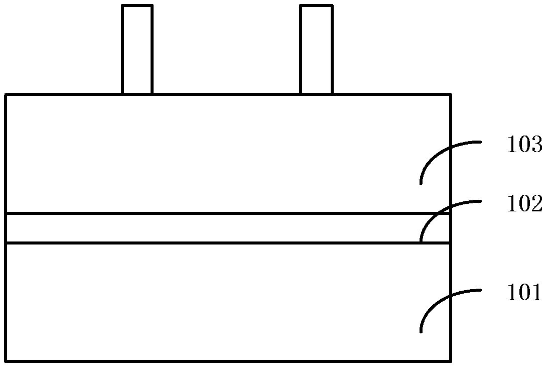
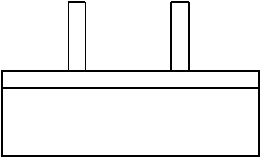
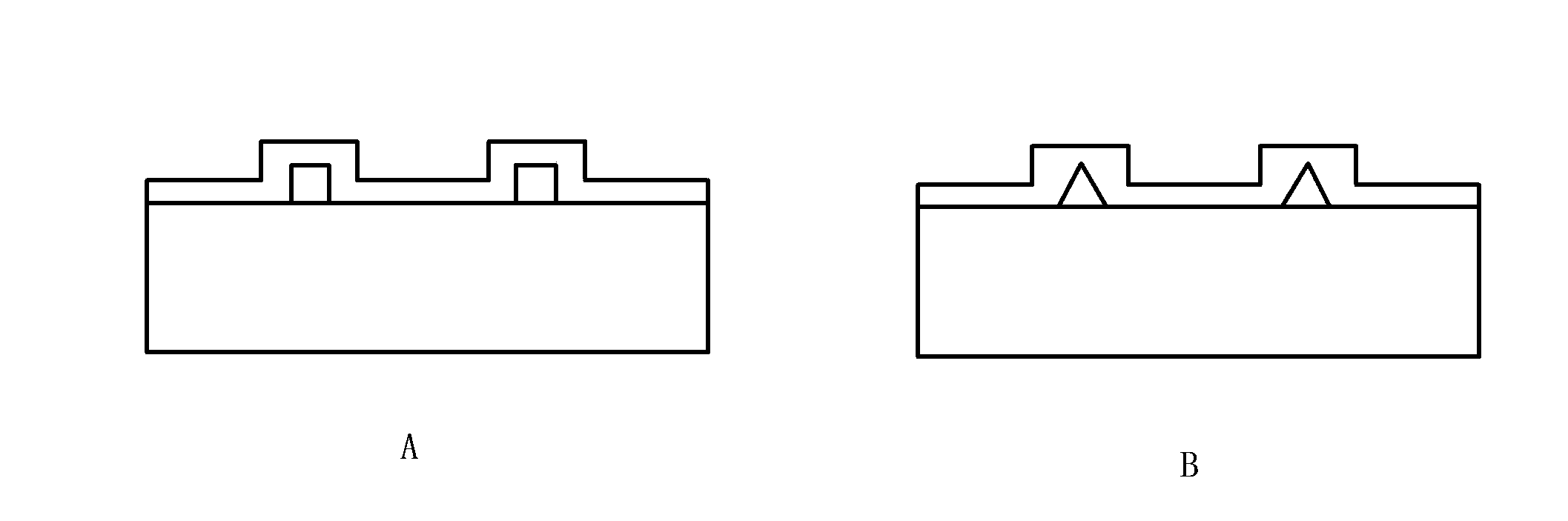
Semiconductor device manufacturing method based on double patterning
A manufacturing method and semiconductor technology, applied in the fields of semiconductor/solid-state device manufacturing, electrical components, photo-engraving process coating equipment, etc., can solve the problems of cumbersome process, device deformation, deformation, etc.
- Summary
- Abstract
- Description
- Claims
- Application Information
AI Technical Summary
Problems solved by technology
Method used
Image

Examples
Embodiment Construction
[0047] In the following description, numerous specific details are set forth in order to provide a more thorough understanding of the present invention. It will be apparent, however, to one skilled in the art that the present invention may be practiced without one or more of these details. In other instances, some technical features known in the art have not been described in order to avoid obscuring the present invention.
[0048]For a thorough understanding of the present invention, a detailed description will be set forth in the following description to illustrate the method of fabricating the semiconductor device of the present invention. Obviously, the practice of the present invention is not limited to the specific details familiar to those skilled in the semiconductor arts. Preferred embodiments of the present invention are described in detail below, however, the present invention may have other embodiments in addition to these detailed descriptions.
[0049] It shoul...
PUM
 Abstract
Description
Claims
Application Information