An adjustable constant current source integrated chip and its manufacturing method
A technology of integrated chip and constant current source, which is applied in semiconductor/solid-state device manufacturing, electric variable adjustment, control/regulation system, etc. It can solve the problems of non-adjustable constant current, high technical level requirements, complex manufacturing process, etc. Achieve the effect of improving the voltage working range, simplifying the process, and good constant current characteristics
- Summary
- Abstract
- Description
- Claims
- Application Information
AI Technical Summary
Problems solved by technology
Method used
Image
Examples
Embodiment 1
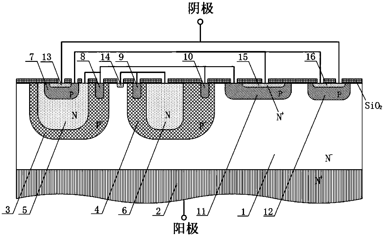
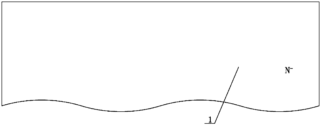
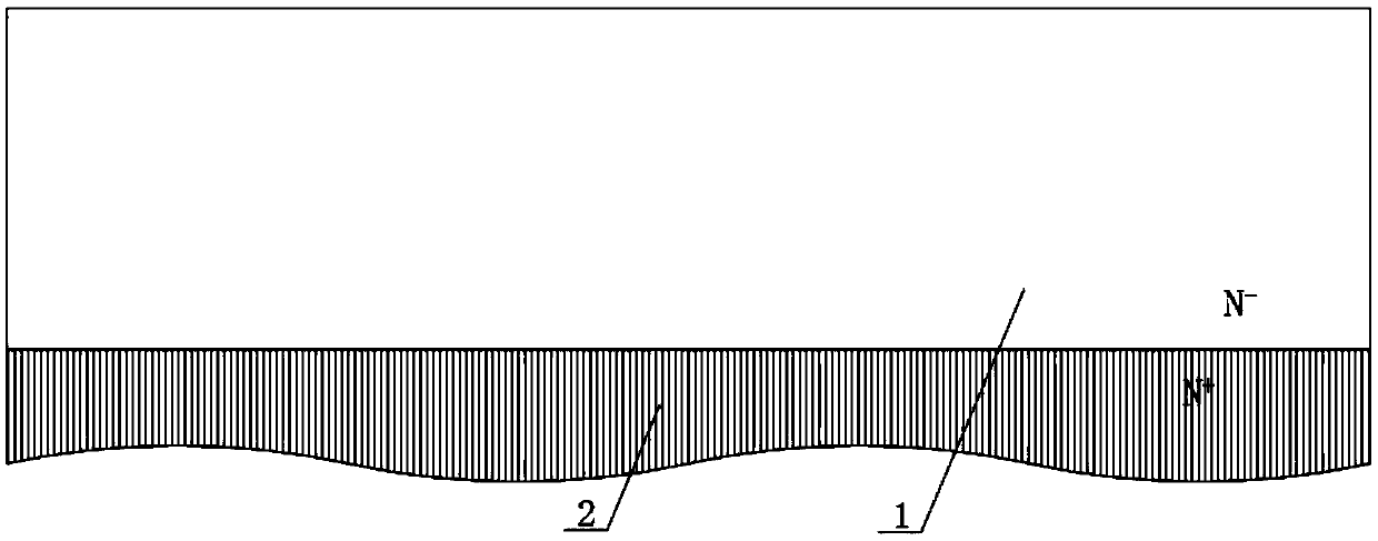
[0054] see figure 1 , the present invention relates to an adjustable constant current source integrated chip, which includes as N - Single crystal silicon N in doped region 1 - type polishing sheet; in the N - The back side of the doped region 1 is provided with N + heavily doped region 2; in the N - The front side of the doped region 1 is provided with the first P of the transistor Q2 - Doped region 3 and the second P of the constant current diode CRD - doped region 4; in the first P - The doped region 3 is doped to form a first N-doped region 5, and in the second P - The second N-doped region 6 is formed by doping on the doped region 4; the first P-doped region 7 is formed on the first N-doped region 5, and the first P - A second P-doped region 8 is formed on the doped region 3, and in the second P - A third P-doped region 9 and a fourth P-doped region 10 are formed on the doped region 4, and the N - The fifth P-doped region 11 of the transistor Q1 and the sixth P-...
Embodiment 2
[0064] Embodiment two, such as Figure 10 As shown, the difference between this embodiment and Embodiment 1 is that the doping types N and P type in the doped region are interchanged, that is, N type becomes P type, P type becomes N type, and the structure is still the same, and finally The functions realized are the same, except that the polarity of the corresponding electrodes is reversed, that is, the front side of the silicon substrate is the anode, and the back side is the cathode. Corresponding to the manufacturing method, only the type of doping impurity is exchanged with that of Embodiment 1, and the process requirements are the same.
PUM
 Abstract
Description
Claims
Application Information


