Tin compound superlattice barrier semiconductor transistor

A superlattice and semiconductor technology, applied in the direction of semiconductor devices, electrical components, circuits, etc., can solve the problems of insufficient smoothness of the barrier layer surface, uneven strain field distribution, and inability to effectively reduce electronic potential energy fluctuations, etc., to achieve smoothness Effects of HEMT morphology, low dislocation density, and high electrical conductivity

Active Publication Date: 2014-05-21
SOUTH CHINA NORMAL UNIVERSITY
View PDF5 Cites 22 Cited by
  • Summary
  • Abstract
  • Description
  • Claims
  • Application Information

AI Technical Summary

Problems solved by technology

Although this patent can increase the two-dimensional electron gas concentration or two-dimensional hole gas concentration in the channel layer, and further increase the driving current of the device, the surface smoothness of the barrier layer is not enough, and the strain between the channel layer Inhomogeneous field distribution, unable to effectively reduce electron potential energy fluctuations

Method used


Image

  • Tin compound superlattice barrier semiconductor transistor
  • Tin compound superlattice barrier semiconductor transistor
  • Tin compound superlattice barrier semiconductor transistor

Examples


Embodiment 1

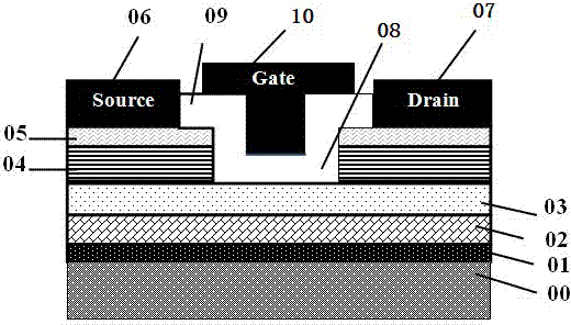
[0028] Such as figure 1 Shown, a kind of tin oxide superlattice barrier semiconductor transistor, its structure comprises:

[0029] High-purity single crystal substrate 00;

[0030] A thin layer of AuO1 evaporated on the single crystal substrate 00;

[0031] A buffer layer 02 formed on a single crystal substrate 00 containing an Au-plated layer 01;

[0032] A high-mobility channel layer 03 formed on the buffer layer 02;

[0033] 5 periods of superlattice barrier layers 04 formed on the high-mobility channel layer 03;

[0034] A narrow bandgap ohmic contact layer 05 formed on the superlattice barrier layer 04;

[0035] A source metal electrode 06 and a drain metal electrode 07 formed on the narrow bandgap ohmic contact layer 05;

[0036] Between the source metal electrode 06 and the drain metal electrode 07, the five-period superlattice barrier layer 04 is etched, and etched to the surface of the high-mobility channel layer 03 to form a gate groove structure 08;

[0037...


PUM

PropertyMeasurementUnit
thicknessaaaaaaaaaa
thicknessaaaaaaaaaa
thicknessaaaaaaaaaa

Abstract

The invention discloses a tin compound superlattice barrier semiconductor transistor, comprising a superlattice barrier layer, wherein the superlattice barrier layer is formed by multi-cycle thin film layers overlapped alternatively, and the thin film layer is composed of tin compound and another doped tin compound. By using the novel compounds of tin and the doping of the tin compounds, a multi-cycle superlattice barrier layer process is formed to obtain low dislocation density, smooth profile of HEMT (High Electron Mobility Transistor), low chip square resistance; the multi-cycle superlattice barrier layer with high conductive performance, high driving current and low MOS (Metal Oxide Semiconductor) interface state density is achieved, and the two-dimensional electron gas concentration or the two-dimensional hole gas concentration in a channel layer is also improved.

Description

technical field [0001] The invention relates to the technical field of semiconductor integrated circuit manufacturing, in particular to a tin oxide superlattice barrier semiconductor transistor. Background technique [0002] Sheet resistance of HEMT chips is one of the important parameters to characterize device performance. Reducing the sheet resistance of HEMT chips is crucial to improving the performance of high-frequency high-power microwave devices. The sheet resistance of the sample depends on the surface electron concentration and electron mobility of the two-dimensional electron gas (2DEG) of the chip, which is determined by the formula [0003] R □ =1 / (μ e no s e) [0004] In the formula, R □ , μ e , n s are the sample sheet resistance, 2DEG electron mobility and areal electron concentration, respectively. [0005] There have been many reports to improve the 2DEG electron mobility and surface electron concentration at the AlGaN / GaN heterojunction interfa...

Claims


Application Information

Patent Timeline
Patent Type & Authority Applications(China)
IPC IPC(8): H01L29/778H01L29/78H01L29/06
CPCH01L29/155H01L29/778
Inventor 赵灵智刘咏梅姜如青李仕杰
Owner SOUTH CHINA NORMAL UNIVERSITY
Why Eureka
Try Eureka