Dual-axis tensile strain GeSn n channel tunneling field effect transistor

A tunneling field effect and transistor technology, which is applied in semiconductor devices, electrical components, circuits, etc., can solve the problems of poor material quality and thermal stability, difficulties, etc., and achieve the effect of increasing tunneling current and improving device performance

Inactive Publication Date: 2014-05-28
CHONGQING UNIV
View PDF3 Cites 5 Cited by
  • Summary
  • Abstract
  • Description
  • Claims
  • Application Information

AI Technical Summary

Problems solved by technology

However, the increase of Sn composition will make the quality and thermal stability of the whole material worse, and it is difficult to obtain GeSn with direct band gap by increasing the composition of Sn

Method used


Image

  • Dual-axis tensile strain GeSn n channel tunneling field effect transistor
  • Dual-axis tensile strain GeSn n channel tunneling field effect transistor
  • Dual-axis tensile strain GeSn n channel tunneling field effect transistor

Examples


Embodiment Construction

[0018] In order to understand the technical essence of the present invention more clearly, the structure and process realization of the present invention are described in detail below in conjunction with the accompanying drawings and embodiments:

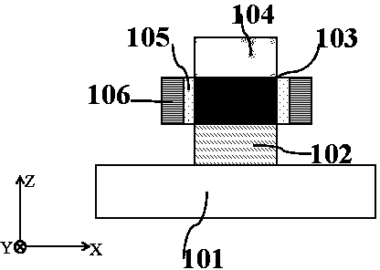
[0019] see figure 1 The biaxial tensile strained GeSn n-channel tunneling field effect transistor is shown, which includes:

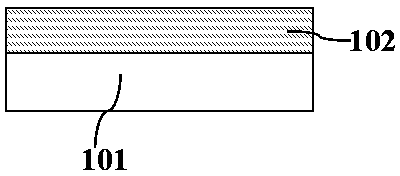
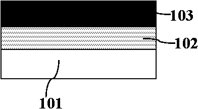
[0020] A substrate 101, the material is single crystal Ge;

[0021] One n channel 103, the material is single crystal GeSn, the general formula is Ge 1-x sn x (0≤ y ≤0.25), if using Ge 0.95 sn 0.05 ;

[0022] A source 102, the material is single crystal GeSn, the general formula is Ge 1-y sn y (0x ≤0.25, x > y ) If Ge can be used 0.9 sn 0.1

[0023] An insulating dielectric film 105 is grown on the channel, such as using H-k (high-k value) material hafnium dioxide H f o 2;

[0024] a gate electrode 106 covering the insulating dielectric film;

[0025] A drain electrode 104 is made of single ...


PUM


Abstract

The invention provides a dual-axis tensile strain GeSn n channel tunneling field effect transistor (10) which structurally comprises a substrate (101), a source electrode (102), a drain electrode (104), a GeSn n channel (103), an insulation dielectric substance film (105) and a grid electrode (106). The source electrode, the n channel and the drain electrode form a vertical device structure. The lattice constant of a regional material of the source electrode is larger than that of the GeSn n channel (103). The GeSn n channel forms dual-axis tensile strain in the X face and the Y face, and the strain facilitates conversion of GeSn of the channel from an indirect band gap into a direct band gap, so that direct quantum tunneling happens, tunneling currents are increased, and device performance is improved.

Description

technical field [0001] The invention relates to a biaxial tensile strained GeSn n-channel TFET (Tunneling Field-effect Transistor: tunneling field-effect transistor). Background technique [0002] With the further development of integrated circuits, the further reduction of chip feature size, and the increase of the number of devices integrated on a single chip, power consumption has become an issue that people pay more and more attention to. According to ITRS data, when the feature size is reduced to the 32nm node, the power consumption will be 8 times the expected trend, that is, with the gradual reduction of the feature size, traditional MOS devices will not be able to meet the demand in terms of power consumption (Nature, vol479, 329-337, 2011). In addition, the reduction in MOSFET size faces the limitation of subthreshold slope at room temperature with a minimum of 60mv / decade. Compared with MOSFETs, tunneling field effect transistors based on quantum tunneling effe...

Claims


Application Information

Patent Timeline
Patent Type & Authority Applications(China)
IPC IPC(8): H01L29/739H01L29/161
CPCH01L29/161H01L29/7391
Inventor 刘艳韩根全王洪娟
Owner CHONGQING UNIV
Why Eureka
Try Eureka