Dual-way growth type carbon nano tube array sensor and preparation method of dual-way growth type carbon nano tube array sensor
A carbon nanotube array and carbon nanotube technology, applied in the direction of material resistance, etc., can solve the problem of gas cannot be adsorbed, and achieve the effect of improved repeatability and excellent electrical contact performance
- Summary
- Abstract
- Description
- Claims
- Application Information
AI Technical Summary
Problems solved by technology
Method used
Image
Examples
Embodiment approach 1
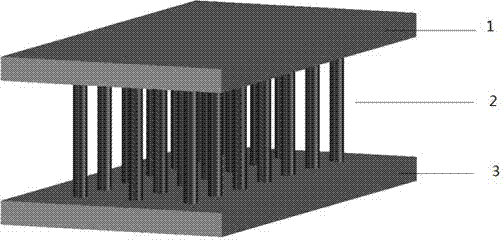
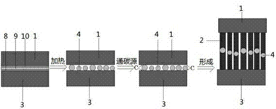
[0047] Embodiment 1: The scheme of the novel array type carbon nanotube sensor of the present invention is as Figure 5 As shown, the preparation steps are as follows:
[0048] ① Use a silicon wafer or other materials as the substrate 5. If the substrate 5 is a conductive material, prepare an insulating layer 6 on the substrate 5 by oxidation or any coating method, and use acetone, ethanol and deionized water to clean it. Remove surface dirt to obtain a clean substrate 5 and insulating layer 6;
[0049] ② Using photolithography technology to prepare photolithographic patterns according to the design requirements on a clean substrate,
[0050] ③ Vacuum coating, sputtering coating or other coating methods are used on the photolithographic substrate, and the buffer layer metal 7 and the bottom electrode layer 3 are sequentially plated on the photolithographic substrate;
[0051] ④ Coating an insulating layer 11 on the previously treated buffer layer metal 7 by sputtering or oth...
Embodiment approach 2
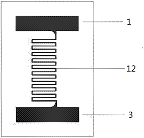
[0057] Embodiment 2: The carbon nanotube sensor of the present invention can also be prepared into a sensor array structure. like Image 6 shown. Multiple groups of carbon nanotube array structures are used, so that each group is modified with different sensitive materials, which can meet the requirements of simultaneous measurement of different types of gases. The preparation process is similar to Embodiment 1:
[0058] ① Use a silicon wafer or other materials as the substrate 5. If the substrate 5 is a conductive material, prepare an insulating layer 6 on the substrate 5 by oxidation or any coating method, and use acetone, ethanol and deionized water to clean it. Remove surface dirt to obtain a clean substrate 5 and insulating layer 6;
[0059] ② Using photolithography technology, the array sensor structure is prepared on a clean substrate.
[0060] ③ Vacuum coating, sputtering coating or other coating methods are used on the photoetched substrate, and the buffer layer met...
PUM
| Property | Measurement | Unit |
|---|---|---|
| diameter | aaaaa | aaaaa |
| width | aaaaa | aaaaa |
| width | aaaaa | aaaaa |
Abstract
Description
Claims
Application Information


