Preparation method of power device

A power device, N-type technology, used in semiconductor/solid-state device manufacturing, semiconductor devices, electrical components, etc., can solve problems such as insufficient injection depth

Active Publication Date: 2014-06-04
INST OF MICROELECTRONICS CHINESE ACAD OF SCI +2
View PDF5 Cites 8 Cited by
  • Summary
  • Abstract
  • Description
  • Claims
  • Application Information

AI Technical Summary

Problems solved by technology

[0007] The technical problem to be solved by the present invention is to provide a preparation method of a power device,

Method used


Image

  • Preparation method of power device

Examples


Embodiment 1

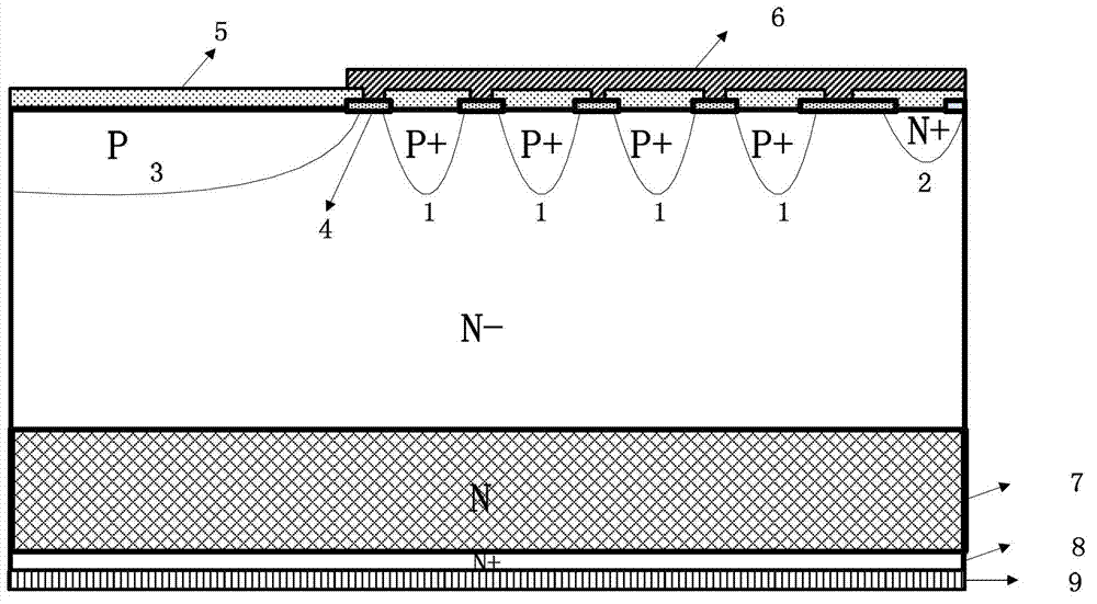
[0030] A method for preparing a FRD structure provided by an embodiment of the present invention includes the following steps:

[0031] Step 101: Substrate preparation, select an N+ type substrate 8 with a thickness of 300um;

[0032] Step 102: Deposit an amorphous silicon field stop layer 7, and deposit an N-type doped amorphous silicon film layer on the upper surface of the N+ type substrate 8 by ion-enhanced chemical vapor phase to form N-type amorphous silicon The field stop layer, wherein the thickness of the N-type doped amorphous silicon thin film layer is 30um, and the doping concentration of the N-type doped amorphous silicon thin film layer is 1e13cm -2 ;

[0033] Step 103: Perform high-temperature annealing on the N-type amorphous silicon field stop layer 7. There are a large number of defects in the epitaxial amorphous silicon film, the carrier recombination coefficient is very high, and the carrier lifetime is very short. Defects can be repaired by high-temperat...

Embodiment 2

[0045] A method for preparing a FRD structure provided by an embodiment of the present invention includes the following steps:

[0046] Step 201: Substrate preparation, select an N+ type substrate with a thickness of 500um;

[0047] Step 202: Deposit an amorphous silicon field stop layer, and deposit an N-type doped amorphous silicon thin film layer on the upper surface of the N+ type substrate 8 by using an ion-enhanced chemical vapor phase method to form an N-type amorphous silicon field stop layer. The cut-off layer, wherein the thickness of the N-type doped amorphous silicon thin film layer is 10um, and the doping concentration of the N-type doped amorphous silicon thin film layer is 5e13cm -2 ;

[0048] Step 203: Perform high-temperature annealing on the N-type amorphous silicon field stop layer. There are a large number of defects in the epitaxial amorphous silicon film, the carrier recombination coefficient is very high, and the carrier lifetime is very short. Defects...

Embodiment 3

[0060] A method for preparing a FRD structure provided by an embodiment of the present invention includes the following steps:

[0061] Step 301: Substrate preparation, select an N+ type substrate with a thickness of 400um;

[0062] Step 302: Deposit an amorphous silicon field stop layer, and deposit an N-type doped amorphous silicon film layer on the upper surface of the N+ type substrate by ion-enhanced chemical vapor deposition to form N-type amorphous silicon The field stop layer, wherein the thickness of the N-type doped amorphous silicon thin film layer is 20um, and the doping concentration of the N-type doped amorphous silicon thin film layer is 5e13cm -2 ;

[0063] Step 303: performing high-temperature annealing on the N-type amorphous silicon field stop layer. There are a large number of defects in the epitaxial amorphous silicon film, the carrier recombination coefficient is very high, and the carrier lifetime is very short. Defects can be repaired by high-temperat...


PUM

PropertyMeasurementUnit
Thicknessaaaaaaaaaa
Thicknessaaaaaaaaaa
Thicknessaaaaaaaaaa

Abstract

The invention discloses a preparation method of a power device, and belongs to the technical field of semiconductors. The method comprises the steps that an N type doped A-Si thin film layer is deposited on the upper surface of an N+ type substrate to form an N type A-Si field stop layer, after high temperature annealing, an N- epitaxial layer is formed on the N type A-Si field stop layer through an eptiaxial method, then an SiO2 thin film layer is formed on the upper surface of the N- eptiaxial layer, an annular area is exposed on the upper surface of the SiO2 thin film layer to form a protecting ring structure of a terminal; an annular area at the outermost periphery is exposed on a stop ring of the terminal, and then N+ type ion implantation and annealing are conducted to form a terminal area. According to the preparation method of the power device, the N type layer is formed through eptiaxial A-Si to be used as a field stop layer of the power device, rest carriers can be combined quickly, outward manifestation is that trailing currents which enable the power device to be shut off are shortened, shut-off time is shortened, and shut-off loss is reduced.

Description

technical field [0001] The invention belongs to the technical field of semiconductors, and in particular relates to a preparation method of a power device. Background technique [0002] Power devices such as IGBT and FRD are widely used in circuit structures such as frequency converters and inverters as necessary switching devices. With the continuous optimization of its structure and performance, its static loss and turn-off loss are continuously reduced, and the topology of the circuit has more and more stringent requirements for its switching loss. High-performance power devices require not only good forward characteristics, but also fast turn-off time. This requirement can be achieved by using life control technology. Lifetime control technology is to speed up the recombination speed of power devices storing charges when they are turned off by doping recombination centers, so as to reduce the turn-off time. Generally, there are two methods of diffusing metal atoms and...

Claims


Application Information

Patent Timeline
IPC IPC(8): H01L21/335H01L21/324H01L21/265
CPCH01L29/04H01L29/0638H01L29/6609
Inventor 吴振兴朱阳军田晓丽卢烁今
Owner INST OF MICROELECTRONICS CHINESE ACAD OF SCI
Why Eureka
Try Eureka