Light emitting diode

A technology for light-emitting diodes and semiconductors, which is applied in thin material processing, semiconductor devices, electrical components, etc. It can solve the problems of reducing luminous intensity and difficult to realize the coalescence of nitride semiconductor layers, so as to increase the recombination rate and reduce the defect density. , the effect of increasing the luminous intensity

Active Publication Date: 2014-05-28
LITE ON TECH CORP
View PDF9 Cites 6 Cited by
  • Summary
  • Abstract
  • Description
  • Claims
  • Application Information

AI Technical Summary

Problems solved by technology

Although upwardly extending dislocations may not be prone to exist in parts of the buffer layer in some practices, since the LED's emission wavelength shifts to the ultraviolet wavelength, the defect density of the LED remains relatively high, and the buffer layer needs to be grown to a certain A thickness (for example, greater than 10 μm), and it is difficult to achieve coalescence of the nitride semiconductor layer, thereby significantly reducing the luminous intensity of the LED at ultraviolet wavelengths

Method used


Image

  • Light emitting diode
  • Light emitting diode
  • Light emitting diode

Examples


Embodiment I

[0082] In this embodiment, by having several quantum barrier layers of an active layer doped with an n-type dopant (where the number of doped quantum barrier layers satisfies a specific relationship), or by having The minimum doping concentration at the quantum barrier layer doped with an n-type dopant close to the p-type semiconductor, or by making the doping concentration of the quantum barrier layer doped with an n-type dopant satisfy a certain relationship, n-type dopants can compensate for the effects of defects on carriers. Accordingly, the recombination rate of carriers of the LED device can be enhanced. Therefore, by using any of the aforementioned techniques, the luminous efficiency of the LED device in the embodiments can be significantly increased in the wavelength range of 222nm to 405nm.

[0083] Figure 11A is an optical simulation diagram of a comparative example of an LED device according to a comparative example in an exemplary embodiment of the present inve...

Embodiment II

[0094] In this embodiment, through one of the three quantum barrier layers closest to the p-type semiconductor layer (which has a thickness greater than that of the other two quantum barrier layers), or the quantum potential in the active layer The thickness of the barrier layer satisfies a specific relationship, the electron-hole pairs can be evenly distributed in the active layer, the probability of electron-hole recombination can be increased, and the luminous intensity of the LED device in the wavelength range of 222nm to 405nm can be significantly improved.

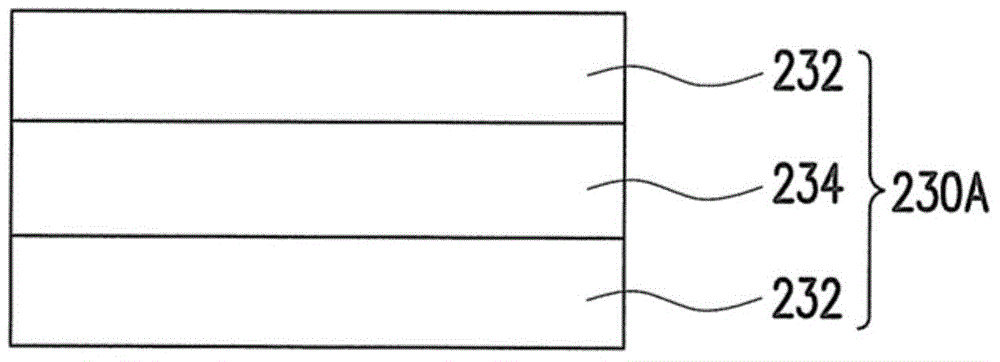
[0095] According to this embodiment, it is assumed that the active layer 230 of the LED device 200 has image 3 The structure shown, and a current of 300mA and a current of 700mA were applied. Under these conditions, the luminous intensity of the LED device 200 is provided in Table 3 when the thickness (unit: nm) of the quantum barrier layers 232 a - 232 f at different positions is changed. Herein, the thickness of ...

Embodiment III

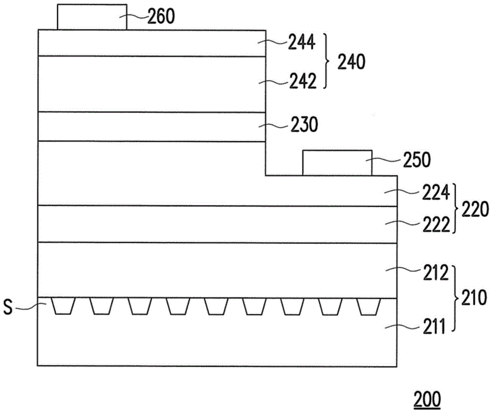
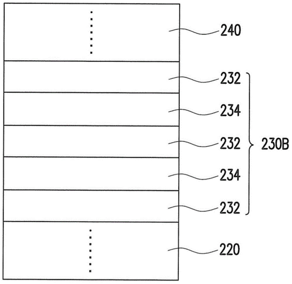
[0111] Figure 14 It is a schematic cross-sectional view of an LED device in an exemplary embodiment of the present invention. Figure 14 The structure of the LED device 300 depicted in is similar to figure 1 LED device 200 is depicted in , except that electron barrier layer 270 and interlayer 280 are located between active layer 230 and p-type semiconductor layer 240 . Figure 15 for Figure 14 An enlarged schematic cross-sectional view of the active layer in the LED device depicted in . Figure 15 The structure of the active layer 230 depicted in is similar to image 3 The structure of the active layer 230 depicted in , except that the order of the quantum barrier layers 232a-232f from the p-type semiconductor layer 240 is 232a, 232b, 232c, 232d, 232e and 232f, and from the p-type semiconductor layer 240 The quantum wells 234a to 234e are counted in sequence as 234a, 234b, 234c, 234d and 234e, and the electron barrier layer 270 and the interlayer 280 are located between...


PUM


Abstract

A light emitting diode device may include a carrier, a p-type and n-type semiconductor layers, an active layer, a first electrode and a second electrode. The carrier has a growth surface and at least one nano-patterned structure on the growth surface, in which the carrier includes a substrate and a semiconductor capping layer disposed between the substrate and the n-type semiconductor layer. The n-type semiconductor layer and the p-type semiconductor layer are located over the growth surface of the carrier. The active layer is located between the n-type and p-type semiconductor layers, in which a wavelength [lambda] of light emitted by the active layer is 222 nm<=[lambda]<=405 nm, and a defect density of the active layer is less than or equal to 5*1010/cm2. The first and second electrodes are respectively connected to the n-type and p-type semiconductor layers. A carrier for carrying a semiconductor layer is also provided.

Description

[0001] Cross References to Related Applications [0002] This application claims the benefit of priority to US Provisional Application No. 61 / 727,090, filed November 15, 2012. The above patent application is hereby incorporated by reference in its entirety and constitutes a part of this specification. technical field [0003] The invention relates to a light-emitting diode (LED) and an LED capable of enhancing luminous intensity. Background technique [0004] For example, a light emitting diode (LED) is a semiconductor device composed primarily of Group III to Group V compound semiconductor materials. These semiconductor materials have the property of converting electricity into light. Therefore, when an electric current is applied to the semiconductor material, the electrons therein will combine with the holes, and excess energy will be released in the form of light, thereby achieving the effect of luminous brightness. [0005] When the luminous wavelength of the LED gr...

Claims


Application Information

Patent Timeline
Patent Type & Authority Applications(China)
IPC IPC(8): H01L33/20H01L33/12H01L33/22H01L33/06
CPCH01L33/12H01L33/20H01L33/007H01L33/025H01L33/06Y10T428/24562H01L33/04H01L33/002H01L33/22H01L33/642
Inventor 傅毅耕宣融刘训志
Owner LITE ON TECH CORP
Why Eureka
Try Eureka