LED quantum well structure, manufacture method of the same, and LED epitaxial wafer comprising the same

A technology of LED epitaxial wafers and manufacturing methods, which is applied in the direction of electrical components, circuits, semiconductor devices, etc., and can solve the problems of low growth temperature of InGaN layers, large polarization effects, and large internal stress of quantum well structures, etc.

Active Publication Date: 2014-09-24
XIANGNENG HUALEI OPTOELECTRONICS
View PDF7 Cites 5 Cited by
  • Summary
  • Abstract
  • Description
  • Claims
  • Application Information

AI Technical Summary

Problems solved by technology

Therefore, the growth temperature of the InGaN layer in the green LED is lower, and the lattice quality in the formed InGaN layer is worse; at the same time, the internal stress in the quantum well structure...

Method used


Image

  • LED quantum well structure, manufacture method of the same, and LED epitaxial wafer comprising the same
  • LED quantum well structure, manufacture method of the same, and LED epitaxial wafer comprising the same
  • LED quantum well structure, manufacture method of the same, and LED epitaxial wafer comprising the same

Examples


Embodiment 1

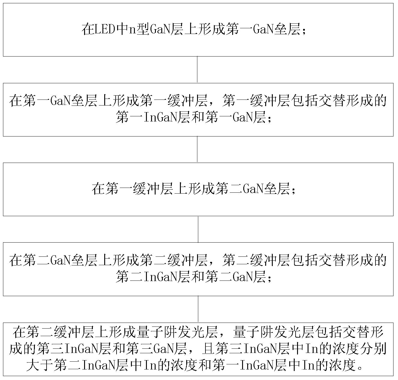
[0065] This embodiment provides a method for manufacturing an LED epitaxial wafer, comprising the following steps:

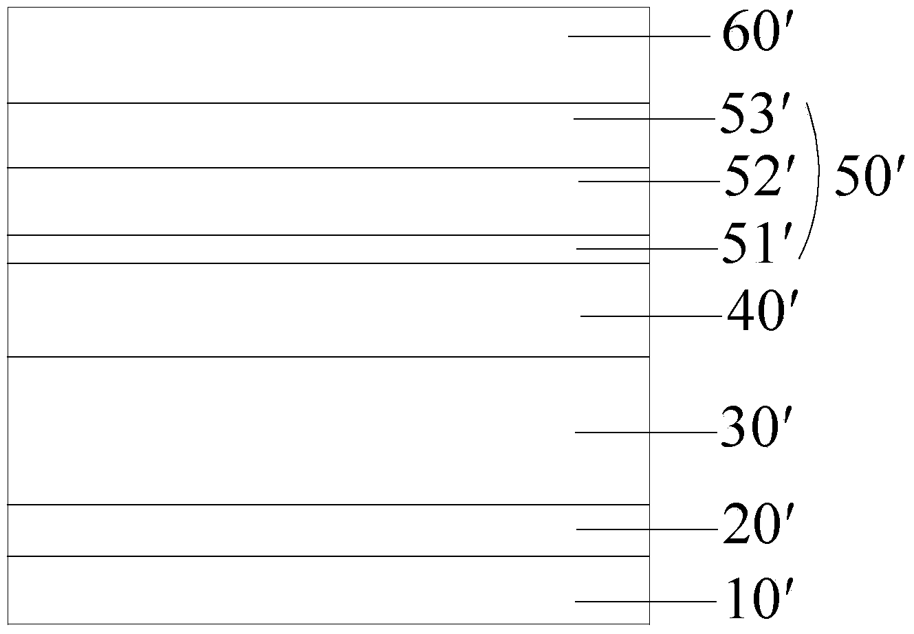
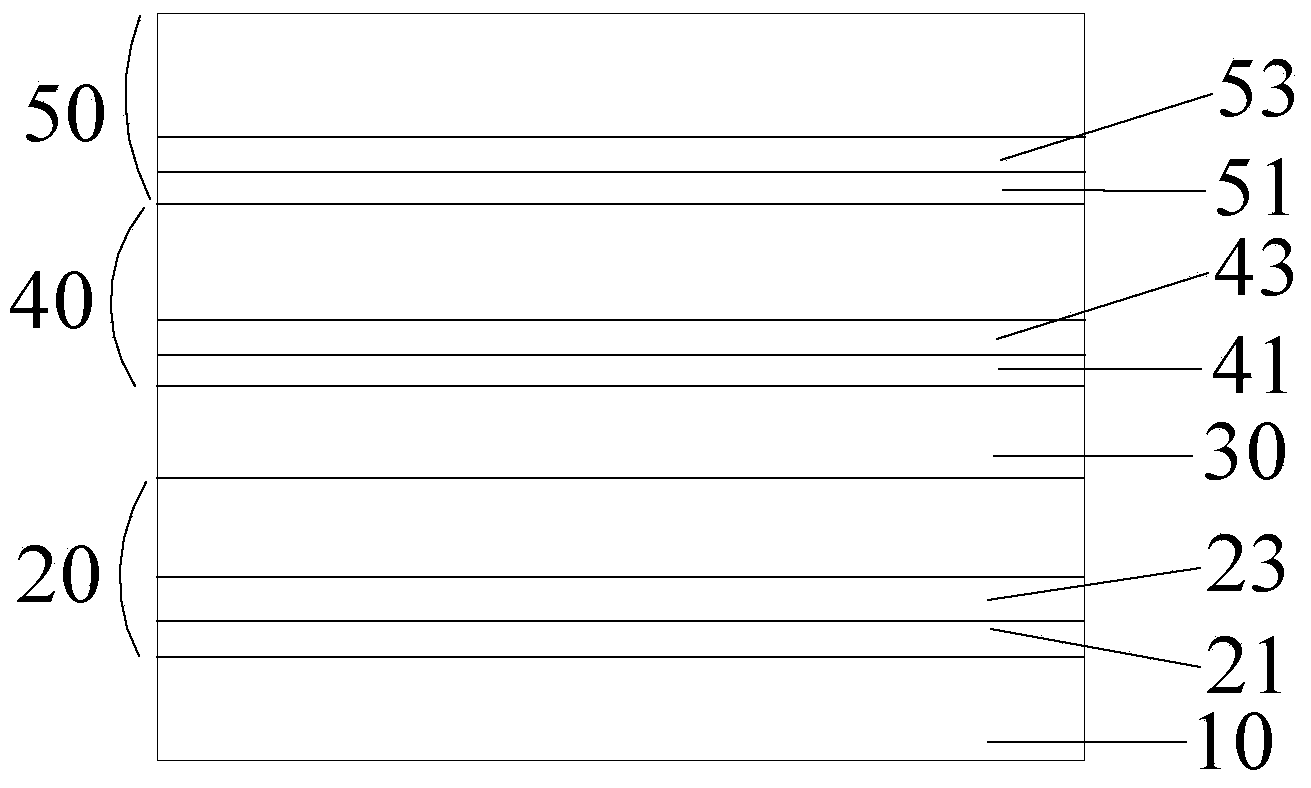
[0066] Forming a GaN buffer layer, u-type GaN, and n-type epitaxial layer includes the following steps: placing the sapphire substrate in an MOCVD reaction chamber, and feeding 100 standard liters / min of high-purity H at a temperature of 1100°C 2 Process the sapphire substrate for 20 minutes; lower the temperature to 570°C, grow a GaN buffer layer with a thickness of 45nm on the sapphire substrate; raise the temperature to 1150°C, grow a 2.5μm u-type GaN layer on the GaN buffer layer; cool down to 1000 ℃, grow a 100nm AlGaN layer on the u-type GaN layer; raise the temperature to 1130 °C, grow a 3.5 μm Si-doped n-type GaN layer on the AlGaN layer, where the doping concentration of Si is 1.5E19atom / cm 3 ;

[0067] Forming the quantum well structure includes the following steps: lower the temperature to 900°C, and grow a first GaN barrier layer with a thickness ...


PUM

PropertyMeasurementUnit
Thicknessaaaaaaaaaa
Thicknessaaaaaaaaaa
Thicknessaaaaaaaaaa

Abstract

The invention discloses an LED quantum well structure, a manufacture method of the same, and an LED epitaxial wafer comprising the same. The structure comprises: a first GaN barrier layer arranged on an n-type GaN layer in an LED; a first buffer layer arranged on the first GaN barrier layer and including a first InGaN layer and a first GaN layer arranged alternately; a second GaN barrier layer arranged on the first buffer layer; a second buffer layer arranged on the second GaN barrier layer and including a second InGaN layer and a second GaN layer arranged alternately; and a quantum well light emitting layer arranged on the second buffer layer and including a third InGaN layer and a third GaN layer arranged alternately. The In concentration of the third InGaN layer is greater than that of the second InGaN layer and greater than that of the first InGaN layer. The crystal quality of the quantum well light emitting layer of the structure is improved.

Description

technical field [0001] The invention relates to the technical field of semiconductor lighting, in particular to an LED quantum well structure, a manufacturing method thereof and an LED epitaxial wafer comprising the quantum well structure. Background technique [0002] Light-emitting diode (LED), as a new type of high-efficiency, environmentally friendly and green solid-state lighting source, has the advantages of small size, light weight, long life, high reliability and low power consumption, making it widely used. In particular, with the rapid development of the LED industry, the application range of green LEDs has gradually expanded, and they are widely used in various fields such as indoor and outdoor large-scale billboards, traffic lights, backlights (computer and mobile phone display screens), and fixed color lighting systems. The market share of LED products related to green light is also expanding year by year, and the market has higher and higher performance require...

Claims


Application Information

Patent Timeline
IPC IPC(8): H01L33/06H01L33/12H01L33/00
CPCH01L33/0075H01L33/06H01L33/12H01L33/32
Inventor 刘为刚曾莹徐迪苗振林
Owner XIANGNENG HUALEI OPTOELECTRONICS
Why Eureka
Try Eureka