How the transistor is formed

A technology of transistors and semiconductors, applied in the direction of semiconductor devices, semiconductor/solid-state device manufacturing, electrical components, etc., can solve the problems that the performance of semiconductor devices has not been significantly improved, and achieve the effects of eliminating short channel effects, stable positions, and enhanced distribution

Active Publication Date: 2016-12-28
SEMICON MFG INT (SHANGHAI) CORP
View PDF8 Cites 0 Cited by
  • Summary
  • Abstract
  • Description
  • Claims
  • Application Information

AI Technical Summary

Problems solved by technology

However, although the method of adjusting the work function of the gate in the prior art improves the short channel effect, the performance of the semiconductor device has not been significantly improved.

Method used


Image

  • How the transistor is formed
  • How the transistor is formed
  • How the transistor is formed

Examples


Embodiment Construction

[0035] The following describes the technical solutions of the present invention clearly and completely through specific embodiments in conjunction with the accompanying drawings. Obviously, the described embodiments are only a part of the implementation manners of the present invention, rather than all of them. According to these embodiments, all other implementation manners that can be obtained by a person of ordinary skill in the art without creative labor fall within the protection scope of the present invention.

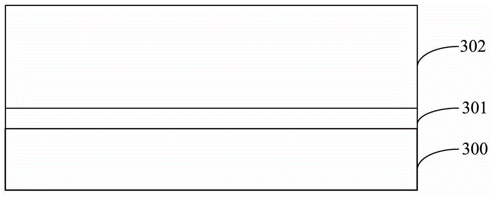
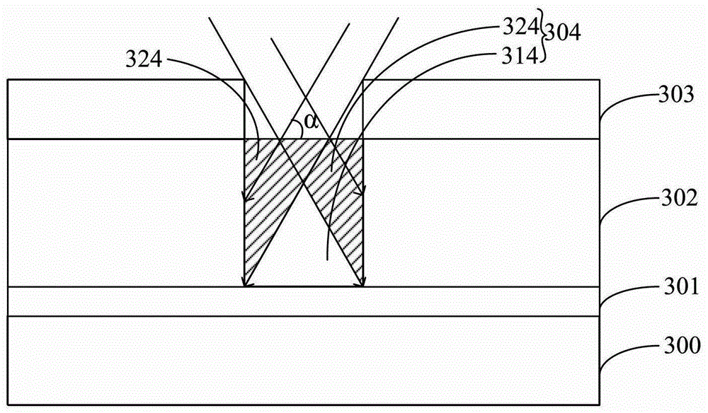
[0036] Reference figure 2 , Combined with reference figure 1 Step S11 is performed to provide a semiconductor substrate 300, on which a dielectric layer 301 and a polysilicon layer 302 located on the dielectric layer 301 are formed.

[0037] In a specific embodiment, the material of the semiconductor substrate 300 may be single crystal silicon, single crystal germanium or single crystal silicon germanium; it may also be silicon-on-insulator (SOI); or may also include ...


PUM

PropertyMeasurementUnit
angleaaaaaaaaaa

Abstract

A forming method of a transistor includes the steps of providing a semi-conductor substrate, wherein a dielectric layer and a polycrystalline silicon layer on the dielectric layer are formed on the semi-conductor substrate; carrying out work function adjustment on the polycrystalline silicon layer to form a work function polycrystalline silicon layer, wherein the work function polycrystalline silicon layer is divided into a first work function area and second work function areas in the grid length direction, the second work function areas are located on the two sides of the first work function area, when the transistor is an NMOS transistor, work functions of the second work function areas are higher than a work function of the first work function area, and when the transistor is a PMOS transistor, the work functions of the second work functions are lower than the work function of the first work function area; removing a polycrystalline silicon layer portion except the work function polycrystalline silicon layer and taking the remaining work function polycrystalline silicon layer as a grid; forming a source electrode and a drain electrode on the semi-conductor substrate on the two sides of the grid. When the transistor is used, the short-channel effect is weakened and even eliminated.

Description

Technical field [0001] The present invention relates to the field of semiconductor technology, in particular to a method for forming a transistor. Background technique [0002] In the field of semiconductor technology, transistors are widely used as the most basic semiconductor devices. During normal operation, the gate electrode is energized, and the electric field generated by the gate voltage controls the generation of carriers in the channel region between the source and drain. When the gate voltage reaches the threshold voltage of the transistor, the source terminal of the channel region is inverted and the carriers in the channel region are allowed to move between the source and drain. For example, when the transistor is an NMOS tube, the gate voltage is a positive voltage, which will attract electrons to move to the gate, thereby forming a conduction channel. However, with the improvement of the element density and integration of semiconductor devices, the gate size of t...

Claims


Application Information

Patent Timeline
Patent Type & Authority Patents(China)
IPC IPC(8): H01L21/336
CPCH01L29/42356
Inventor 鲍宇
Owner SEMICON MFG INT (SHANGHAI) CORP
Why Eureka
Try Eureka