Semiconductor test structure and test method thereof

A test structure, semiconductor technology, applied in the direction of semiconductor/solid-state device testing/measurement, semiconductor devices, semiconductor/solid-state device components, etc., can solve the problem of ineffective detection of double damascene structure defects, double damascene structure is easy to form defects, and affects SRAM Memory stability and other issues, to achieve the effect of simple test method, space saving and high efficiency

Active Publication Date: 2014-06-04
SEMICON MFG INT (SHANGHAI) CORP
View PDF7 Cites 2 Cited by
  • Summary
  • Abstract
  • Description
  • Claims
  • Application Information

AI Technical Summary

Problems solved by technology

[0006] The existing dual damascene structure is formed by the electroplating process, but with the continuous reduction of the feature size, defects are easily formed in t

Method used


Image

  • Semiconductor test structure and test method thereof
  • Semiconductor test structure and test method thereof
  • Semiconductor test structure and test method thereof

Examples


Embodiment Construction

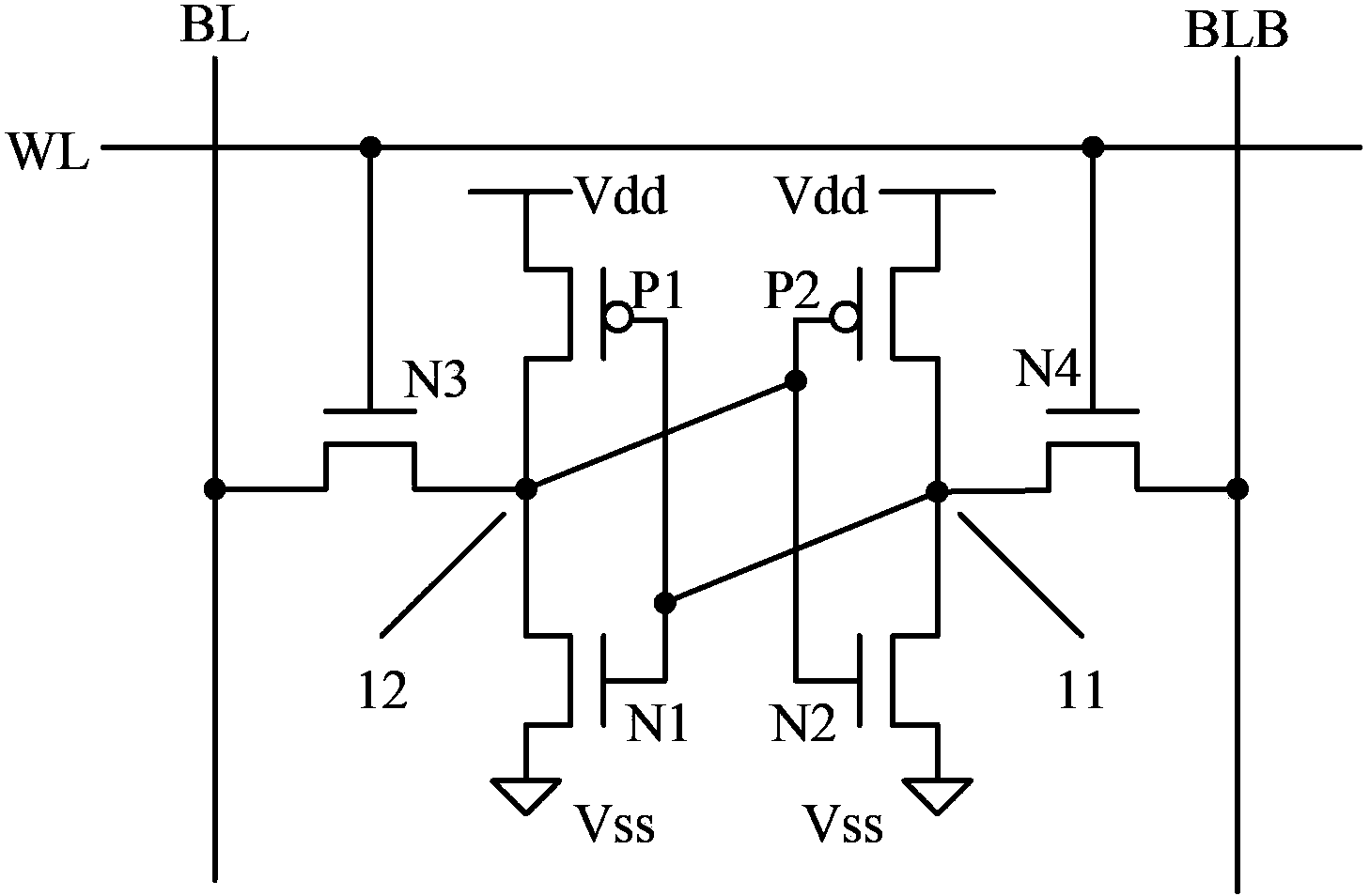
[0038] The inventor found in the existing process of making SRAM memory that the electroplating process is used to form a dual damascene structure for connecting metal interconnection lines, word lines and bit lines with the gate, source or drain of transistors in memory cells. At this time, due to the continuous reduction of feature size, it is easy to form defects such as voids in the dual damascene structure. The existence of defects such as voids will affect the electrical performance of the dual damascene structure, and ultimately affect the stability of the SRAM memory of the formed semiconductor device.

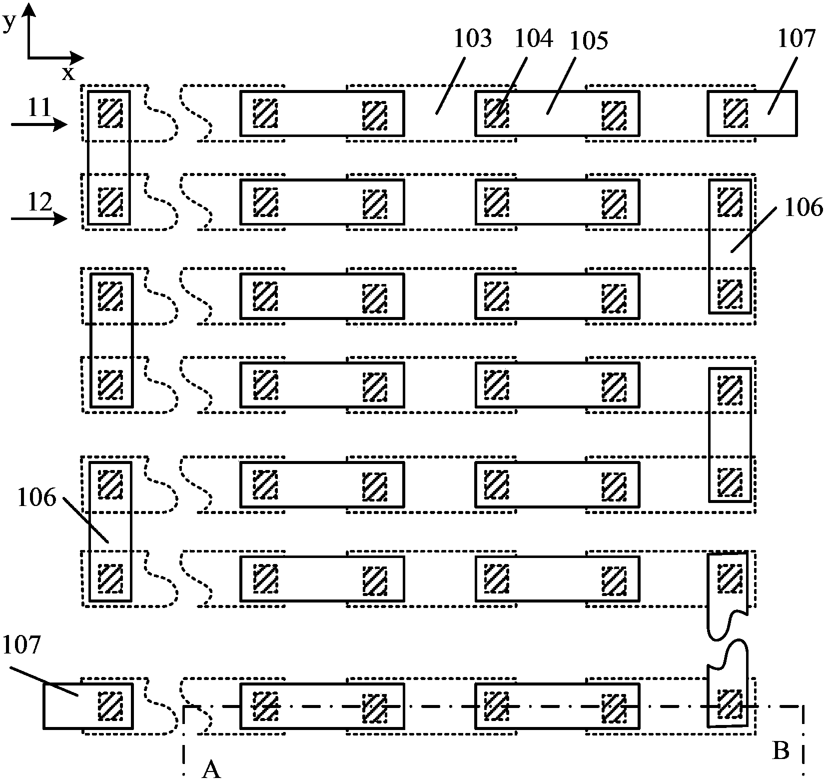
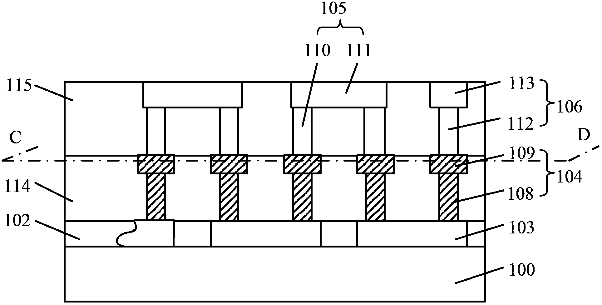
[0039] The inventors have further studied and found that when forming a dual damascene structure, it is necessary to form through holes and grooves connected to the through holes in the dielectric layer, and when filling metal copper in the grooves and through holes, the size and arrangement direction of the grooves, It will have a great impact on the filling performanc...


PUM


Abstract

The invention discloses a semiconductor test structure and a test method of the semiconductor test structure. The semiconductor test structure is formed in the mode that a plurality of dually-embedded structures which are distributed in rows and columns form a plurality of sub test chains connected in series, the head ends of the sub test chains are connected with one another, the tail ends of the sub test chains are connected with one another, and therefore the sub test chains are connected in series to form the semiconductor test structure. According to the semiconductor test structure and the test method of the semiconductor test structure, space is saved; by means of testing the resistance of the semiconductor test structure, whether the dually-embedded structures have defects is judged; the test method is simple, and test efficiency is high.

Description

technical field [0001] The invention relates to the field of semiconductor manufacturing, in particular to a semiconductor testing structure and a testing method thereof. Background technique [0002] Static random access memory (SRAM), as a member of volatile memory, has the advantages of high speed, low power consumption and compatibility with standard processes, and is widely used in PCs, personal communications, consumer electronics (smart cards, digital cameras, multimedia players ) and other fields. [0003] figure 1 It is a schematic diagram of the circuit structure of the storage unit of the existing 6T structure SRAM memory, the storage unit includes: a first PMOS transistor P1, a second PMOS transistor P2, a first NMOS transistor N1, a second NMOS transistor N2, and a third NMOS transistor N3 and the fourth NMOS transistor N4, the first PMOS transistor P1, the second PMOS transistor P2, the first NMOS transistor N1, and the second NMOS transistor N2 form a bistab...

Claims


Application Information

Patent Timeline
IPC IPC(8): H01L23/544H01L21/66
Inventor 白凡飞鲍宇
Owner SEMICON MFG INT (SHANGHAI) CORP
Why Eureka
Try Eureka