

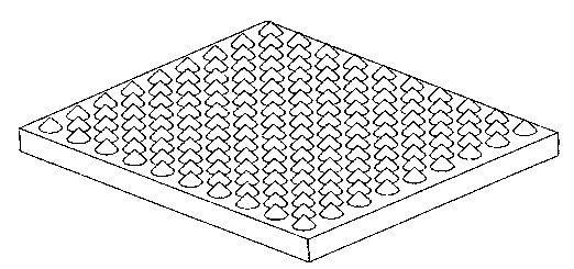
Method for fast preparing sapphire pattern substrate through nanoimprint technology
A technology of nanoimprinting and graphic substrates, which is applied in the direction of optomechanical equipment, photolithography of patterned surfaces, optics, etc., can solve the problems affecting the performance and quality of internal quantum efficiency chips, substrate graphic design and improvement limitations, lining In order to improve the internal quantum efficiency and light extraction efficiency, improve the yield rate of the chip, reduce the effect of reverse leakage and electrostatic breakdown
- Summary
- Abstract
- Description
- Claims
- Application Information
AI Technical Summary
Problems solved by technology
Method used
Image

Examples
Embodiment Construction
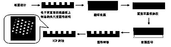
[0027] Imprint lithography can be divided into step-by-step imprint and full-sheet imprint according to the imprint area; it can be divided into thermal imprint lithography and room temperature imprint lithography (UV -NIL); according to the hardness of the imprint mold, it can be divided into soft imprint lithography and hard imprint lithography.
[0028] The preparation method of the present invention comprises the steps:
[0029] (1) There are two ways to prepare nanoimprint templates: hard template and soft template.
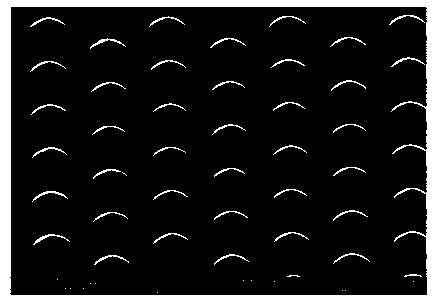
[0030] (2) Grow an epitaxial layer on a clean sapphire substrate, and evaporate SiO2 or Cr to obtain the target sheet.
[0031] (3) The surface of the target piece is coated with an appropriate amount of hot pressing glue.
[0032] (4) Imprint the target sheet after uniform glue with the nanoimprint template.
[0033] (5) Transfer the surface pattern of the photoresist to the surface of the target sheet.
[0034] (6) Through a series of post-processing, ...
PUM
 Abstract
Description
Claims
Application Information