Forming method of fin-type field effect transistor

A fin-type field effect and transistor technology, which is applied in semiconductor devices, semiconductor/solid-state device manufacturing, electrical components, etc., and can solve problems such as high process costs

Active Publication Date: 2014-06-11
SEMICON MFG INT (SHANGHAI) CORP
View PDF7 Cites 12 Cited by
  • Summary
  • Abstract
  • Description
  • Claims
  • Application Information

AI Technical Summary

Problems solved by technology

But the epitaxial growth process needs very high process cost

Method used


Image

  • Forming method of fin-type field effect transistor
  • Forming method of fin-type field effect transistor
  • Forming method of fin-type field effect transistor

Examples


Embodiment Construction

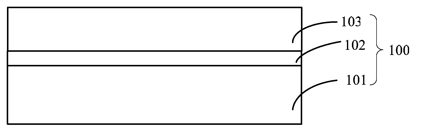
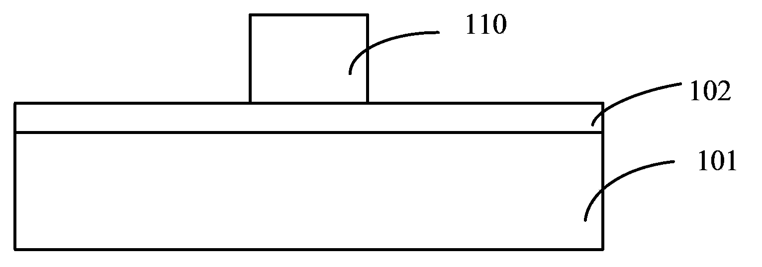
[0027] As mentioned in the background art, as the feature size of transistors shrinks continuously, the mobility of carriers also decreases, so that the saturation current of transistors decreases. However, the existing technology of using SiGe or SiC as the source and drain requires a large process cost.

[0028] The forming method of the Fin Field Effect Transistor proposed by the present invention forms a polysilicon layer by annealing after forming an amorphous silicon layer in the source and drain regions, so as to generate tensile stress on the trench region, improve the mobility of electrons in the NMOS channel region, and improve the transistor performance. performance.

[0029] In order to make the above objects, features and advantages of the present invention more comprehensible, specific implementations of the present invention will be described in detail below in conjunction with the accompanying drawings. The described embodiments are some, but not all, of the p...


PUM


Abstract

A forming method of a fin-type field effect transistor comprises the steps that a semiconductor substrate is provided; a fin portion is formed on the surface of the semiconductor substrate, wherein the fin portion comprises a channel area located between source and drain areas at the two ends of the fin portion; the source and drain areas of the fin portion are etched to enable the height of the source and drain areas to be reduced; non-crystalline silicon layers are formed on the surfaces of the etched source and drain areas; annealing is conducted on the non-crystalline silicon layers to form polycrystalline silicon layers, wherein the polycrystalline silicon layers generate pull stress to the channel area of the fin portion. By means of the method, the migration rate of electrons in a channel of the fin-type field effect transistor can be increased, and the performance of the N-shaped fin type field effect transistor can be improved.

Description

technical field [0001] The invention relates to the technical field of semiconductors, in particular to a method for forming a fin field effect transistor. Background technique [0002] With the continuous development of semiconductor process technology, the process node is gradually reduced, and the gate-last (gate-last) process has been widely used to obtain an ideal threshold voltage and improve device performance. However, when the feature size (CD, Critical Dimension) of the device is further reduced, even the field effect transistor manufactured by the gate-last process can no longer meet the demand for device performance, and multi-gate devices have gained widespread attention. [0003] Fin field effect transistor (Fin FET) is a common multi-gate device, figure 1 A three-dimensional schematic diagram of a fin and a gate structure of a fin field effect transistor in the prior art is shown. Such as figure 1 As shown, it includes: a semiconductor substrate 10, a protr...

Claims


Application Information

Patent Timeline
Patent Type & Authority Applications(China)
IPC IPC(8): H01L21/336
CPCH01L21/02532H01L21/02592H01L21/02667H01L29/66795
Inventor 三重野文健
Owner SEMICON MFG INT (SHANGHAI) CORP
Why Eureka
Try Eureka