Semiconductor device and manufacturing method thereof

A manufacturing method, semiconductor technology, applied in the direction of semiconductor/solid-state device manufacturing, semiconductor devices, electric solid-state devices, etc., can solve problems such as unsuitable for batch production, complex process of semiconductor device methods, high cost, etc., to achieve easy mass production, save Effect of de-deposition step and mask and etch step, suppression of random fluctuations

Active Publication Date: 2014-06-11
INST OF MICROELECTRONICS CHINESE ACAD OF SCI
View PDF5 Cites 22 Cited by
  • Summary
  • Abstract
  • Description
  • Claims
  • Application Information

AI Technical Summary

Problems solved by technology

Therefore, the method for manufacturing a semiconductor device including a double metal gate and a d

Method used


Image

  • Semiconductor device and manufacturing method thereof
  • Semiconductor device and manufacturing method thereof
  • Semiconductor device and manufacturing method thereof

Examples


Embodiment Construction

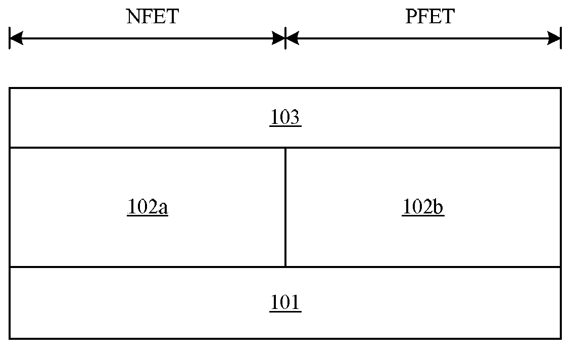
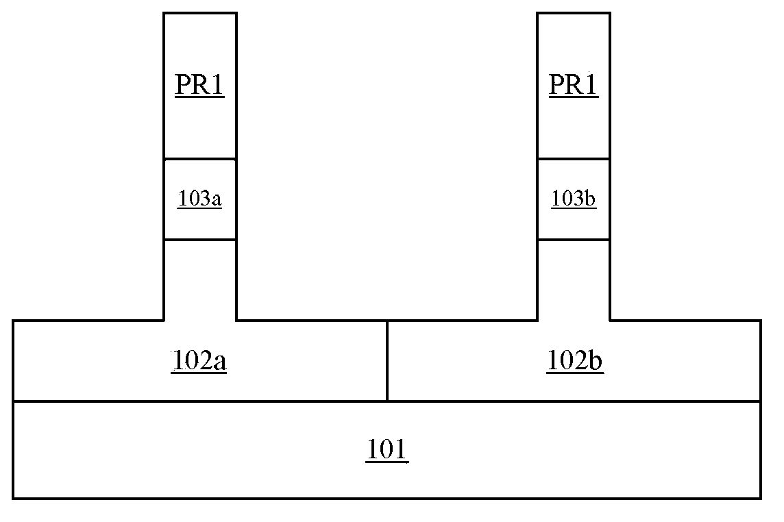
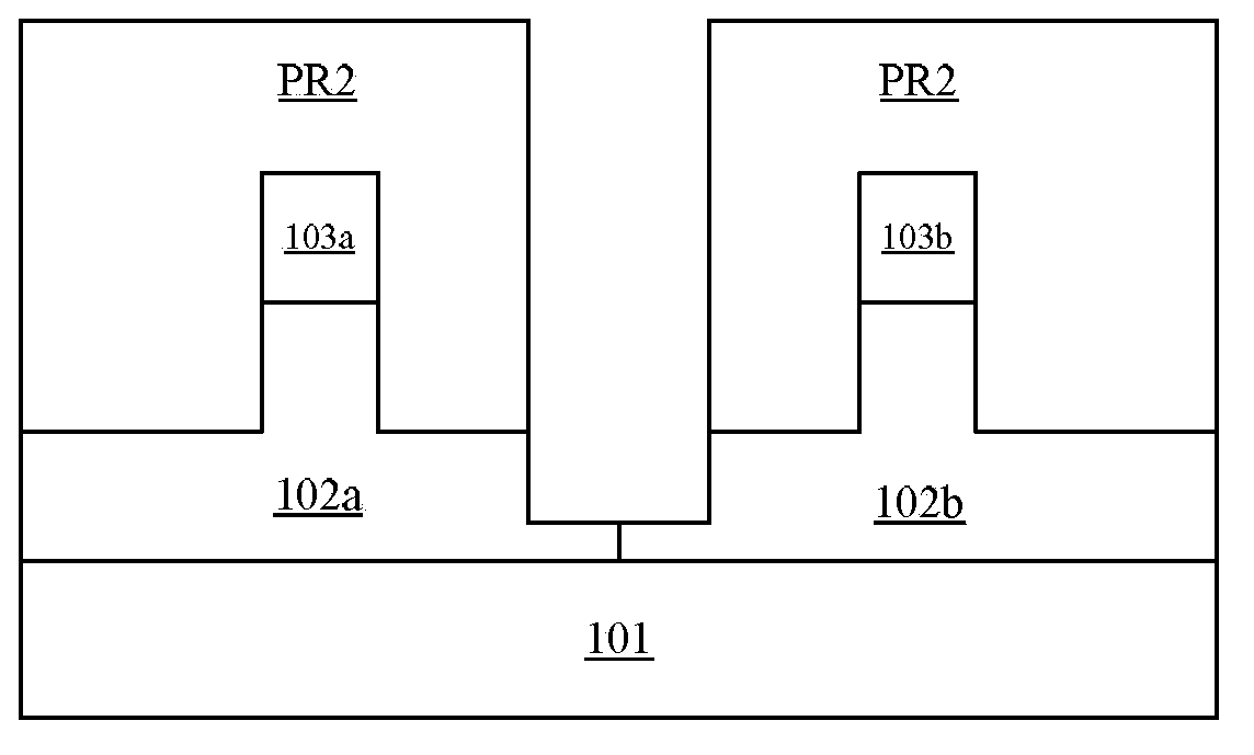
[0011] Hereinafter, the present invention will be described in more detail with reference to the accompanying drawings. In the following description, similar components are denoted by the same or similar reference numerals whether they are shown in different embodiments or not. In the various drawings, for the sake of clarity, various parts in the drawings are not drawn to scale.

[0012] In the following, many specific details of the present invention are described, such as device structures, materials, dimensions, processing techniques and techniques, for a clearer understanding of the present invention. However, the invention may be practiced without these specific details, as will be understood by those skilled in the art. Unless otherwise specified below, each part in the semiconductor device may be composed of materials known to those skilled in the art, or materials having similar functions developed in the future may be used.

[0013] In the present application, the ...


PUM


Abstract

The invention discloses a semiconductor device and a manufacturing method thereof. The manufacturing method of the semiconductor device includes the following steps that: semiconductor fins are formed on a semiconductor substrate; interfacial oxide layers are formed on the surfaces of the tops and side walls of the semiconductor fins; high K gate dielectrics are formed on the interfacial oxide layers; first metal gate layers are formed on the high K gate dielectrics; and doping agents are implanted into the first metal gate layers through conformal doping; and annealing is performed, so that the doping agents can be diffused and accumulated at upper interfaces between the high K gate dielectrics and the first metal gate layers and lower interfaces between the high K gate dielectrics and the interfacial oxide layers, and electric dipoles can be generated at the lower interfaces between the high K gate dielectrics and interfacial oxides through interfacial reaction.

Description

technical field [0001] The invention relates to the field of semiconductor technology, in particular to a semiconductor device including a metal gate and a high-K gate dielectric and a manufacturing method thereof. Background technique [0002] With the development of semiconductor technology, the feature size of Metal Oxide Semiconductor Field Effect Transistor (MOSFET) keeps decreasing. The scaling down of MOSFETs leads to a serious problem of gate current leakage. The use of a high-K gate dielectric makes it possible to increase the physical thickness of the gate dielectric while keeping the equivalent oxide thickness (EOT) constant, thereby reducing the gate tunneling leakage current. However, conventional polysilicon gates are not compatible with high-K gate dielectrics. The use of metal gates and high-K gate dielectrics can not only avoid the depletion effect of polysilicon gates, reduce gate resistance, but also avoid boron penetration and improve device reliability...

Claims


Application Information

Patent Timeline
IPC IPC(8): H01L21/8238H01L21/336H01L27/092H01L29/78
CPCH01L29/78H01L21/823821H01L27/0924H01L29/66795H01L21/28088H01L21/28185H01L29/4966H01L29/517H01L29/66545H01L29/785H01L21/28176H01L21/823842H01L21/2652H01L29/1083H01L29/42372H01L29/45H01L29/66537H01L29/6681H01L29/7851
Inventor 朱慧珑徐秋霞张严波杨红
Owner INST OF MICROELECTRONICS CHINESE ACAD OF SCI
Why Eureka
Try Eureka