Forming method for metal gate

A technology of metal gates and gate trenches, which is applied in the fields of electrical components, semiconductor/solid-state device manufacturing, semiconductor devices, etc., can solve problems such as gaps in metal gates and difficulties in the fill process, so as to reduce resistance and solve the manufacturing process The effect of the puzzle

Active Publication Date: 2014-06-18
SEMICON MFG INT (SHANGHAI) CORP
View PDF3 Cites 10 Cited by
  • Summary
  • Abstract
  • Description
  • Claims
  • Application Information

AI Technical Summary

Problems solved by technology

[0007] The technical problem to be solved by the present invention is the difficulty of the gap fill process and the problem of gaps appearing inside the metal gate

Method used


Image

  • Forming method for metal gate
  • Forming method for metal gate
  • Forming method for metal gate

Examples


Embodiment 1

[0048] In this embodiment, NMOS transistors and PMOS transistors are formed by using the first method for forming metal gates, and this embodiment will be described in detail below with reference to the accompanying drawings.

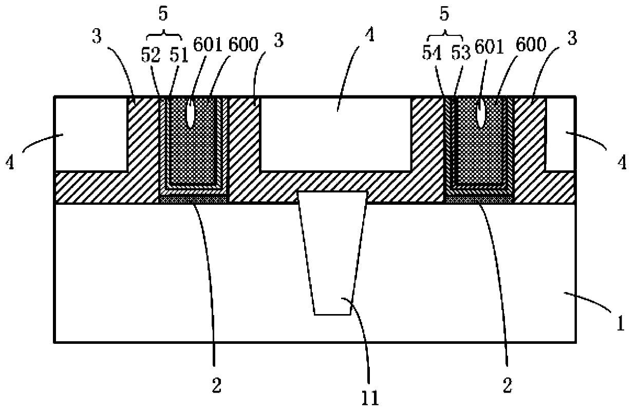
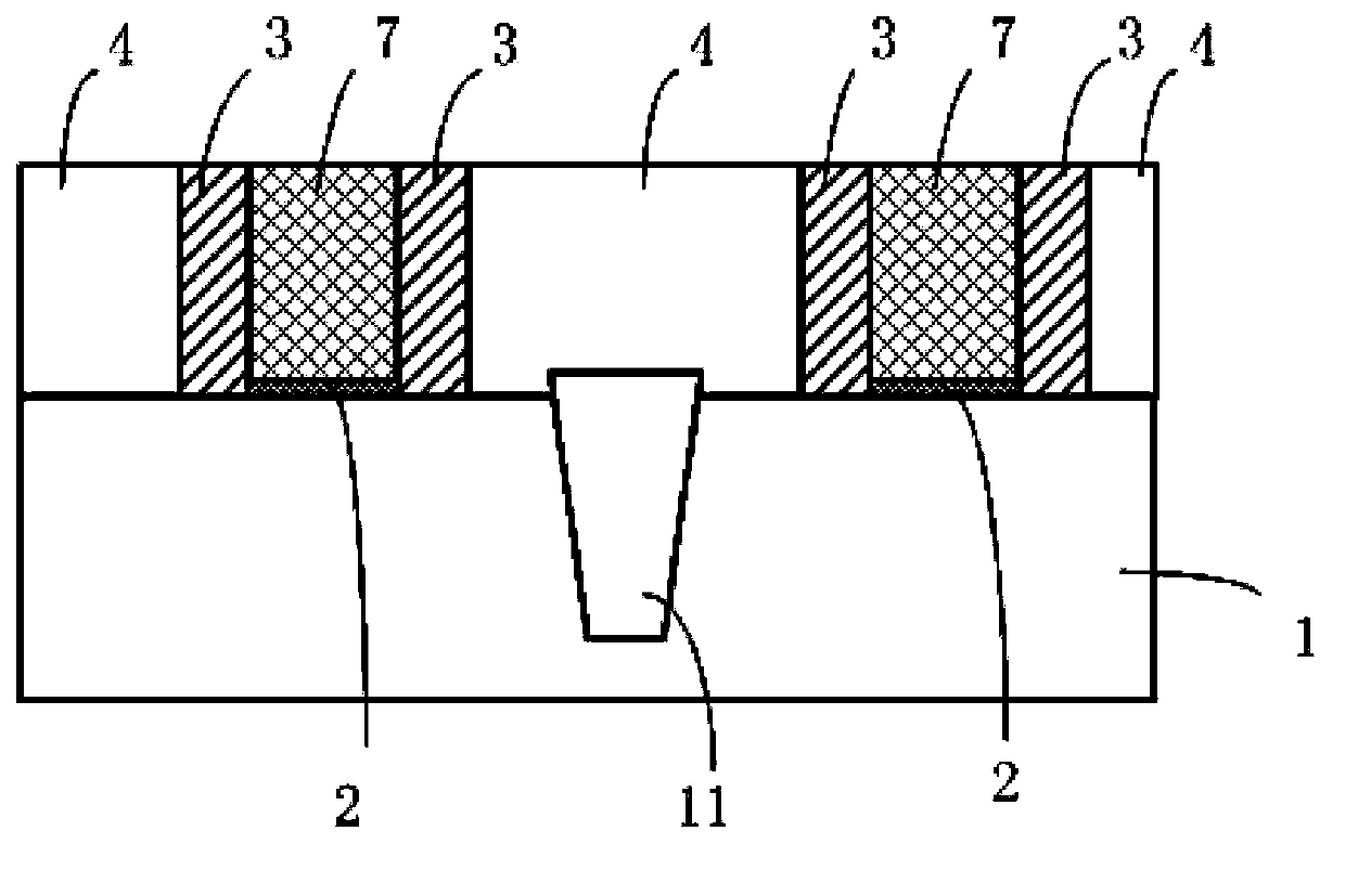
[0049] Please refer to figure 2 Firstly, a dummy gate layer 7 is formed on the substrate 1 , and spacers 3 are formed on both sides of the dummy gate layer 7 .

[0050] The substrate 1 in this embodiment may typically be a silicon substrate, such as a wafer. The silicon substrate can be made of silicon that reaches the purity of the semiconductor industry, or a silicon substrate doped with a small amount of elements such as germanium and / or carbon. The substrate 1 may also be doped with impurity dopant elements such as boron, phosphorus or arsenic. In other embodiments, alternative materials may be used to form the substrate 1, and the alternative materials may or may not be combined with silicon, including but not limited to germanium, indium antimo...

Embodiment 2

[0093] In this embodiment, NMOS transistors and PMOS transistors are fabricated using a method similar to that of Embodiment 1. Most of the steps in this embodiment are the same as those in Embodiment 1. This specification mainly describes the special steps in this embodiment. For other parts, please refer to Embodiment 1. For the content of this embodiment, you can refer to the corresponding figures in Embodiment 1, and at the same time refer to Figure 14 to Figure 16 .

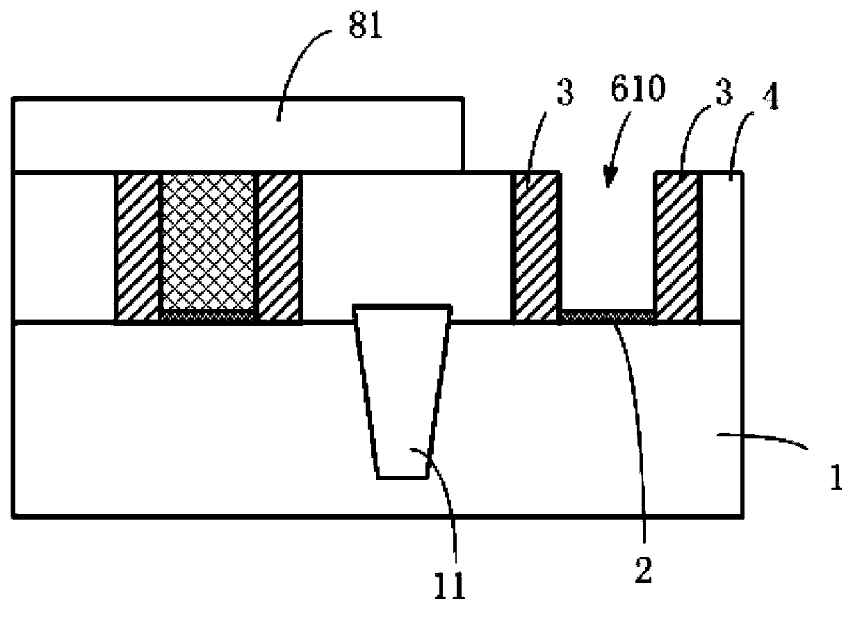
[0094] This embodiment firstly provides the figure 2 The structure shown, then according to embodiment one from Figure 3 to Figure 5 Each step is processed. in getting Figure 5 After the structure shown, what follows is not as Figure 6 Shown to etch the work function metal layer, but take the Figure 5 The first protective mask layer 81 is removed for the structure in , and a third protective mask layer is formed to cover the structures on the right side of the shallow trench isolation region 11 (...

Embodiment 3

[0100] In this embodiment, a method similar to that of Embodiment 1 is used to fabricate a MOS transistor, and for the same part as the previous forming method, reference may be made to the content of the above corresponding part of this specification. The differences will be described in detail below. Please refer to the corresponding figures of the metal gate formation method in the first embodiment, and Figure 17 to Figure 23 .

[0101] This method includes steps S1 to S7, each step will be described in detail below.

[0102] S1 , forming a dummy gate layer 7 on the substrate 1 , and forming sidewalls 3 on both sides of the dummy gate layer 7 .

[0103] The substrate 1 in this embodiment may typically be a silicon substrate 1 such as a wafer. The silicon substrate 1 can be made of silicon with the purity of the semiconductor industry, or a silicon substrate 1 doped with a small amount of elements such as germanium and / or carbon. The substrate 1 may also be doped with i...


PUM


Abstract

The invention provides a forming method for a metal gate. The forming method comprises the following steps of forming a pseudo gate layer on a substrate, and forming sidewalls on the two sides of the pseudo gate layer; removing the pseudo gate layer to form a gate trench between the sidewalls; depositing work function metal to form work function metal layers on the bottom of the gate trench and the sidewalls, and enclosing a groove by using the work function metal layers on the bottom of the gate trench and the sidewalls; forming a protective layer to fill the groove, and performing flattening; etching the work function metal layer on the sidewalls of the gate trench to form a recess; removing the protective layer to connect the groove with the recess to form a nick; depositing a metal material to fill the nick. According to the forming method for the metal gate, an opening filled with the metal gate material is enlarged by a corresponding process step, so that gaps in the formed metal gate are avoided.

Description

technical field [0001] The invention relates to the field of semiconductor manufacturing, in particular to a method for forming a metal gate. Background technique [0002] The main device in an integrated circuit, especially a VLSI, is a metal oxide semiconductor field effect transistor (MOS transistor for short). Since the MOS tube was invented, its geometric size has been continuously reduced. In this context, various practical and fundamental limitations and technical challenges begin to emerge, and further scaling down of device dimensions is becoming more and more difficult. As the manufacturing process of Complementary Metal-Oxide-Semiconductor (CMOS, Complementary Metal-Oxide-Semiconductor) shrinks to a level below 32nm, technologies using new designs and materials are introduced. [0003] Among them, in the fabrication of MOS transistor devices and circuits, the most challenging thing is that the traditional CMOS devices are shrinking due to polysilicon / SiO 2 Or t...

Claims


Application Information

Patent Timeline
Patent Type & Authority Applications(China)
IPC IPC(8): H01L21/28
CPCH01L21/823828H01L29/401H01L29/66545
Inventor 韩秋华孟晓莹
Owner SEMICON MFG INT (SHANGHAI) CORP
Why Eureka
Try Eureka