Chemical mechanical grinding method applied to FinFET (fin field-effect transistor) structure

A chemical-mechanical and grinding method technology, applied in electrical components, semiconductor/solid-state device manufacturing, circuits, etc., can solve problems such as nitride removal defects, and achieve the effect of simple and easy method.

Inactive Publication Date: 2014-06-18
SHANGHAI HUALI MICROELECTRONICS CORP
View PDF8 Cites 4 Cited by
  • Summary
  • Abstract
  • Description
  • Claims
  • Application Information

AI Technical Summary

Problems solved by technology

However, the patent still has the

Method used


Image

  • Chemical mechanical grinding method applied to FinFET (fin field-effect transistor) structure
  • Chemical mechanical grinding method applied to FinFET (fin field-effect transistor) structure
  • Chemical mechanical grinding method applied to FinFET (fin field-effect transistor) structure

Examples


Embodiment Construction

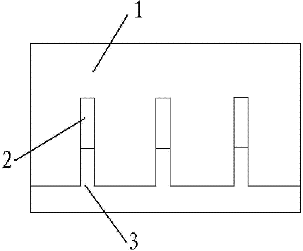
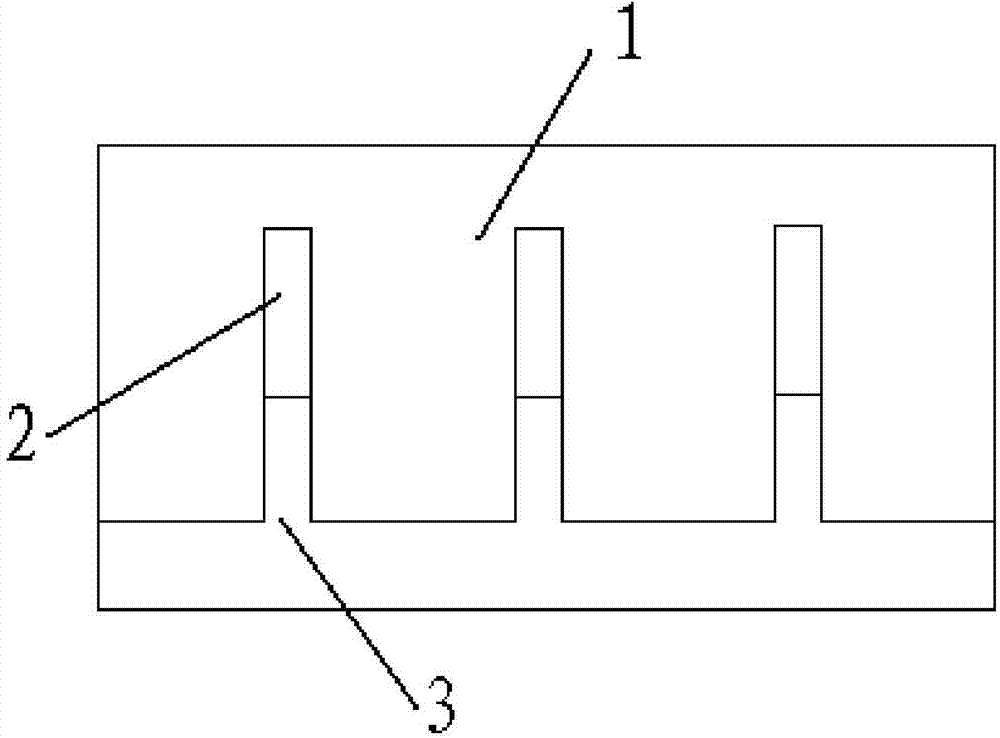
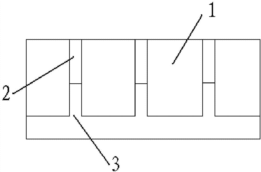
[0030] The invention provides a chemical mechanical polishing method applied to a FINFET structure, which uses a CMP process and adds an endpoint detection method, so that the grinding can completely remove silicon nitride and stop on the oxide layer of the buffer pad, so as to completely remove nitrogen by using the CMP process For the purpose of silicon nitride, there is no need for wet removal of silicon nitride. This endpoint detection method is to use the change of motor torque current caused by the change of wafer surface friction before and after silicon nitride removal, so as to collect the torque current signal and capture the sudden change that stops on the buffer oxide layer after grinding and removing silicon nitride. Signal point to achieve the effect of grinding stop.

[0031] The method of the present invention will be described in detail below in conjunction with the accompanying drawings.

[0032] A chemical mechanical polishing method applied to a FINFET str...


PUM


Abstract

The invention provides a chemical mechanical grinding method applied to a FinFET (fin field-effect transistor) structure. The chemical mechanical grinding method comprises the steps of grinding oxide on silicone nitride; grinding the oxide and the silicone nitride, and collecting torque current signals of a motor; when the torque current signals suddenly change, grabbing a final grinding point, and stopping on a buffer cushion oxide layer; providing a certain amount of grinding time for completing grinding and forming the FinFET structure. The technical scheme is simple and feasible, the silicone nitride can be completely removed by utilizing chemical mechanical grinding, and the grinding action is stopped on the buffer cushion oxide layer, so that the effect of removing the silicone nitride without a wet method and removing the oxide without wet etching/dry etching is achieved.

Description

technical field [0001] The invention relates to the field of semiconductor manufacturing, in particular to a chemical mechanical polishing method applied to a FINFET structure. Background technique [0002] The FinFET is called a Fin Field-Effect Transistor (Fin Field-Effect Transistor; FinFET) and is a new complementary metal oxide semiconductor (CMOS) transistor. Fin means fish fin, and FinFET is named according to the similarity between the shape of the transistor and the fish fin. [0003] At present, the existing technology forms FinFET by CMP. After the first step of conventional STI (shallow trench isolation)-CMP is completed, the second step uses dry etch (dry etching) to etch a certain amount of oxide ( Oxide), the third step uses H3PO4 to remove Nitride (nitride) on the active region, and the fourth step uses wet etch (wet etching) to etch a certain amount of oxide, and finally forms a FinFET structure. [0004] In this integration scheme, when Nitride remove (ni...

Claims


Application Information

Patent Timeline
IPC IPC(8): H01L21/336H01L21/3065H01L21/304
CPCH01L29/66795H01L21/31053H01L21/67253
Inventor 丁弋朱也方严钧华王从刚
Owner SHANGHAI HUALI MICROELECTRONICS CORP
Why Eureka
Try Eureka