DFM (design for manufacturability) method for territory

A technology of layout and graphics, applied in the DFM field of layout, can solve the problem of ignoring the determination of local area pattern density, and achieve the effect of reducing difficulty, eliminating influence and easy manufacturing

Active Publication Date: 2014-06-18
SHANGHAI HUAHONG GRACE SEMICON MFG CORP
View PDF8 Cites 11 Cited by
  • Summary
  • Abstract
  • Description
  • Claims
  • Application Information

AI Technical Summary

Problems solved by technology

However, the common dummy filling method has the following problems: it pays more attention to satisfying the requirements of the global graphics density after filling, while ignoring the density determination of the local area graphics
[0006] 1. Lower graphics density

Method used


Image

  • DFM (design for manufacturability) method for territory
  • DFM (design for manufacturability) method for territory
  • DFM (design for manufacturability) method for territory

Examples


Embodiment Construction

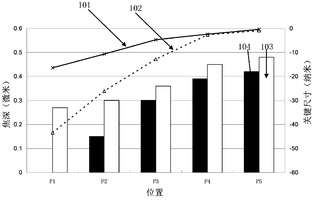
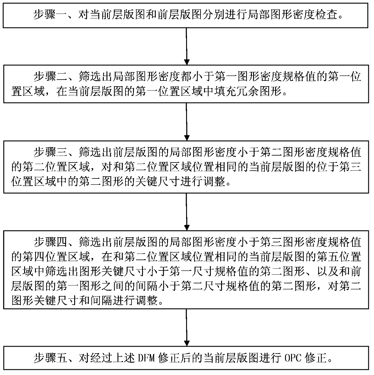
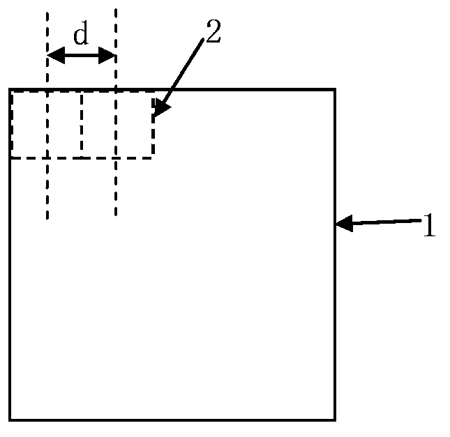
[0053] Such as figure 2 Shown is the flow chart of the DFM method of the layout of the embodiment of the present invention; as Figure 3A to Figure 3G Shown is a schematic diagram of the layout in each step of the method of the embodiment of the present invention. The DFM method of the layout in the embodiment of the present invention is used to perform DFM correction on the design layout. The design layout includes multi-layer layouts, and each DMF correction is performed on one layer of the layout. This layer layout is the current layer layout, and the current layer layout The layout of the previous layer is the layout of the front layer, and the first pattern of the layout of the front layer will form a step on the silicon wafer, and the height of the step is > Typical value is The first pattern may be the formation pattern of the active region (Active Layer) or gate (Poly Layer), etc., and the DFM method uses the following steps to perform DFM correction on the curr...


PUM


Abstract

The invention discloses a DFM (design for manufacturability) method for a territory. The method comprises the following steps that a current layer territory and a former layer territory are respectively subjected to local pattern density inspection; each region with the local pattern density being smaller than a first image density specification value is screened out, and redundant patterns are filled in the regions; the region, with the local image density being smaller than a second image density specification value, of the former layer territory is screened out, and the CD (critical dimension) of the patterns in the same region of the current layer territory is regulated; the region, with the local pattern density being smaller than a third image density specification value, of the former layer territory is screened out, a second image with the pattern CD being smaller than a minimum specification value and the interval from the images of the former layer territory being smaller than a minimum distance specification value is screened out in the same region of the former layer territory, and the CD and the intervals are regulated; the corrected current layer territory is subjected to OPC (optical proximity correction). The DFM method has the advantages that the former layer image influence can be eliminated, and the photoetching process difficulty is reduced, so the design territory can be easily manufactured.

Description

technical field [0001] The present invention relates to a semiconductor integrated circuit manufacturing process method, in particular to a layout design (Design for Manufacturing, DFM) method suitable for industrial production. Background technique [0002] With the development of ultra-large-scale semiconductor integrated circuit manufacturing technology, the number of transistors per unit area is continuously increasing, and the size of a corresponding single transistor is continuously shrinking. The mainstream patterning technology is mainly realized by photolithography. With the continuous shrinking of the design size, the transistor size is getting closer and closer to the limit of optical resolution. At this time, many small changes in process parameters will have an impact on the photolithography pattern. Process parameters such as exposure energy, focal length, exposure wavelength, and numerical aperture are known, but many other parameters are ignored. Among the...

Claims


Application Information

Patent Timeline
Patent Type & Authority Applications(China)
IPC IPC(8): H01L21/70
CPCH01L22/20H01L27/0207
Inventor 王雷
Owner SHANGHAI HUAHONG GRACE SEMICON MFG CORP
Why Eureka
Try Eureka