Piezoelectric film bulk acoustic resonator and preparation method thereof

A bulk acoustic wave resonator and piezoelectric thin film technology, applied in the direction of electrical components, impedance networks, etc., can solve the problems of reducing the electrical performance of the device, increasing the manufacturing cost and process complexity of the device, so as to avoid over-throwing of the sacrificial layer and meet high requirements. The effect of high frequency and large Q value

Inactive Publication Date: 2014-06-18
UNIV OF ELECTRONIC SCI & TECH OF CHINA
View PDF3 Cites 61 Cited by
  • Summary
  • Abstract
  • Description
  • Claims
  • Application Information

AI Technical Summary

Problems solved by technology

At present, the improved device structure still has disadvantages such as: 1. After the sacrificial layer is deposited, high-precision CMP equipment is required for long-term grinding, which increases the cost and process complexity of

Method used


Image

  • Piezoelectric film bulk acoustic resonator and preparation method thereof
  • Piezoelectric film bulk acoustic resonator and preparation method thereof
  • Piezoelectric film bulk acoustic resonator and preparation method thereof

Examples


specific Embodiment approach

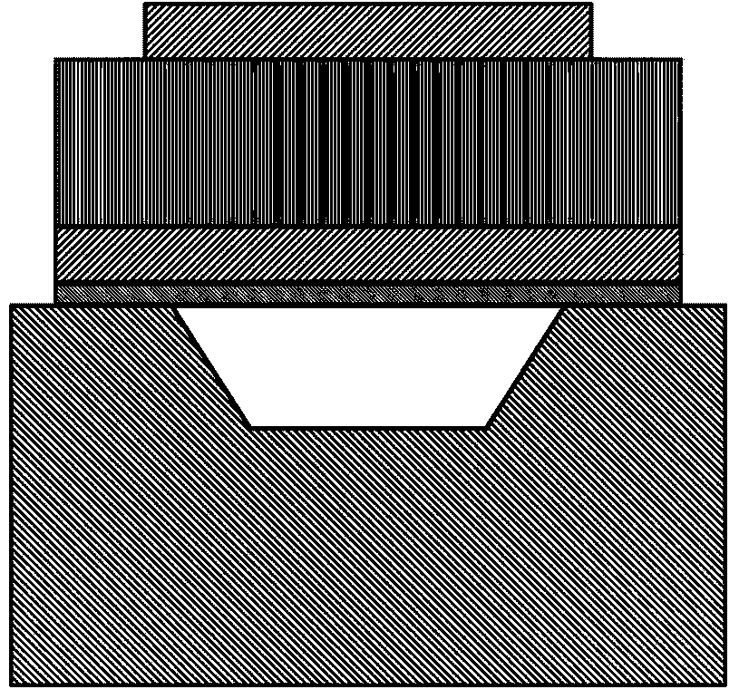
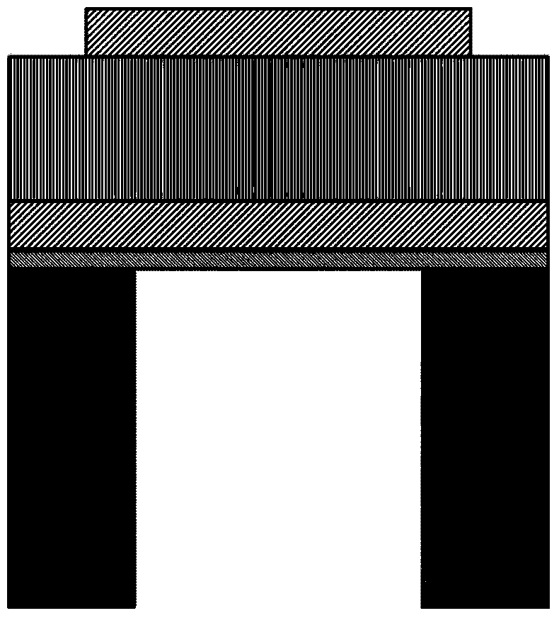
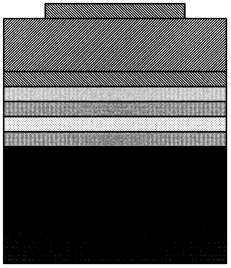
[0050] 1. Use photolithography on the surface of the silicon substrate to remove the photoresist corresponding to the region of the sacrificial layer to expose the silicon substrate. Use dry etching to etch the exposed silicon substrate, the etching depth can be between 200nm-3μm, such as Figure 4 shown. The surface of the silicon substrate may be in (100), (110) or (111) orientation.

[0051] 2. Deposit the amorphous silicon sacrificial layer by electron beam evaporation, and the thickness of the sacrificial layer can be controlled at 300nm-3μm. The sacrificial layer has a temperature greater than 100°C, a deposition rate of less than 5 ? / s, and a background vacuum of less than 10 -3 Deposited under the condition of Pa. The thickness of the sacrificial layer is controlled by the deposition time, as Figure 5 shown.

[0052] 3. Use acetone to dissolve the remaining photoresist on the substrate. When the photoresist is dissolved, the amorphous silicon film layer attached ...


PUM

PropertyMeasurementUnit
Depthaaaaaaaaaa
Etching depthaaaaaaaaaa
Thicknessaaaaaaaaaa

Abstract

The invention discloses a piezoelectric film bulk acoustic resonator and a preparation method thereof. The resonator comprises a substrate, an air cavity, a bottom electrode layer, a piezoelectric layer and a top electrode layer, wherein grapheme is used as the electrode layers of the device; a support layer is not needed in the structure of the device, and the air cavity is formed between the grapheme bottom electrode layer and a groove of the substrate; the piezoelectric layer is arranged on the bottom electrode layer, and the top electrode layer is arranged on the piezoelectric layer. A preparation process of a sacrificial layer is adopted, so the dependence of the traditional process on high-precision chemical-mechanical polishing equipment is overcome, the grinding time is shortened, and the flat surface of sacrificial layer is quickly obtained. The piezoelectric film bulk acoustic resonator has the advantages that the structure is novel, the high Q (quality) value and high electromechanical coupling coefficient can be obtained, and the piezoelectric film bulk acoustic resonator can be applied to the manufacturing of filters, duplexes and multiplexes in subsequent radio frequency communication systems, and can also be combined with different sensitive films to manufacture high-performance sensors.

Description

technical field [0001] The invention belongs to the technical field of radio frequency micro-electromechanical systems, and in particular relates to a novel piezoelectric film bulk acoustic wave resonator and a preparation method thereof. Background technique [0002] In recent years, with the development of wireless communication systems, more and more functions are required to be integrated into the same system. The development trend of multi-function and miniaturization of wireless communication system puts forward the requirements of miniaturization, integration, high application frequency, high performance and low manufacturing cost for the radio frequency devices used in it. With the continuous development of radio frequency micro-electromechanical manufacturing technology, thin-film bulk acoustic resonators based on piezoelectric effects have gradually become the solution for wireless communication system filter chips due to their excellent performance. Compared with...

Claims


Application Information

Patent Timeline
IPC IPC(8): H03H9/17H03H3/02
Inventor 张睿钟慧成英楠石玉焦向全杨杰赵宝林何泽涛
Owner UNIV OF ELECTRONIC SCI & TECH OF CHINA
Why Eureka
Try Eureka