A method of making multi-layer microwave circuits using ceramic substrates

A technology of ceramic substrates and microwave circuits, which is applied in the manufacture of multilayer circuits, circuits, electrical components, etc., can solve the problems of easy fracture of metal layers, large differences in thermal expansion coefficients, and difficult metallization of through holes, etc. Controllable, high implementation precision, good cutting effect

Active Publication Date: 2016-09-28
成都博芯联科科技有限公司
View PDF4 Cites 0 Cited by
  • Summary
  • Abstract
  • Description
  • Claims
  • Application Information

AI Technical Summary

Problems solved by technology

The main disadvantages are that through-hole metallization is difficult, time-consuming, and costly. The reason is that the PTFE material is non-conductive. To metallize its surface, the material must first be chemically activated, and then electroplated and activated; The thermal expansion coefficient of the metal used for the via hole and the substrate material is very different, and the metal layer is easy to break and cause the circuit to be disconnected; the heat dissipation performance of the polytetrafluoroethylene material is poor, which is not suitable for high-power applications, and the surface cannot be mounted with chips

Method used


Image

  • A method of making multi-layer microwave circuits using ceramic substrates
  • A method of making multi-layer microwave circuits using ceramic substrates

Examples


Embodiment 1

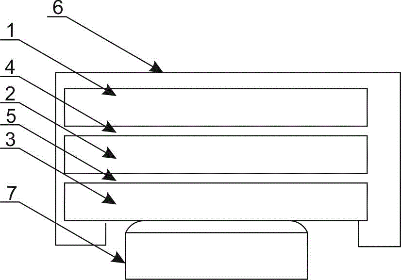
[0026] The ceramic substrate 2 is selected, and a through hole is made on it, and the through hole can be obtained by mechanical or laser drilling. The upper filling board 1 , the ceramic substrate 2 and the lower filling board 3 are stacked sequentially from top to bottom, and the upper filling board 1 and the lower filling board 3 can be made of ceramics. The lower filling plate 3 is provided with a filling port vertically corresponding to the through hole. The sizes of the through hole and the filling port are both in the micron order, but the size of the through hole is larger than that of the filling port, and the radius of the filling port is less than half of the radius of the through hole. one.

[0027] There is a gap 1 between the upper filling plate 1 and the ceramic substrate 2, and there is a gap 2 5 between the ceramic substrate 2 and the lower filling plate 3. The height of the gap 1 4 and the gap 2 5 is 1-20 mm. The first gap 4 and the second gap 5 are used to ...

Embodiment 2

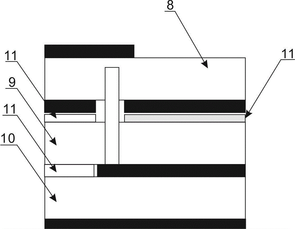
[0034] Fabrication of Microwave Circuits on Three-Layer Ceramic Substrates

[0035] Corresponding through holes are opened on the first ceramic substrate 8 and the second ceramic substrate 9, and the upper filling plate 1 and the lower filling plate 3 are used to fill the through holes of the two ceramic substrates 2 with metal. Make circuit diagrams on the first layer of ceramic substrate 8 and the third layer of ceramic substrate 10, then coat photoresist 11, and remove the photoresist 11 at the through hole, then the three ceramic substrates are superimposed and heated to The metal is melted so that the three layers of ceramic substrates are connected through holes, so as to realize the electrical connection between the first layer and the third layer.

Embodiment 3

[0037] The above-mentioned embodiment 1 provides a method for manufacturing a multilayer microwave circuit, in which the liquid metal in the liquid metal tank 6 needs to be pressed into the through hole of the ceramic substrate 2 . In the present invention, the through hole and the filling port can be cylindrical, and the filling port can be trapezoidal. When the liquid metal rises into the through hole, the pressure difference between the inside of the ceramic substrate 2 and the external atmospheric pressure is greater than twice the ratio of the surface tension coefficient of the liquid metal to the radius of the filled hole. When the through hole is filled, the inside of the ceramic substrate 2 and the outside The pressure difference at atmospheric pressure is less than the ratio of the surface tension coefficient of the liquid metal to the radius of the filled pores.


PUM

PropertyMeasurementUnit
heightaaaaaaaaaa
thicknessaaaaaaaaaa

Abstract

The invention discloses a method for manufacturing a multi-layer microwave circuit by using ceramic substrates. The method comprises the following steps: forming through holes in the ceramic substrates; filling the through holes with liquid metal by means of pressure difference; manufacturing circuits on single layer ceramic substrates; melting the metal in the through holes in the overlapped multi-layer ceramic substrates to connect the through holes in each layer of ceramic substrate. The manufacturing method provided by the invention is controllable in technological process and high in implementation accuracy, and can be used for manufacturing multi-layer microwave circuits containing different ceramic materials. The pressures in the ceramic substrates are adjusted, the liquid metal in a metal liquid groove is pressed into the through holes in the ceramic substrates by means of the pressure difference from the external atmosphere pressure, and the internal pressure intensity is raised automatically, so that the liquid metal between a filling port and the metal liquid groove falls naturally, high filling speed, high filling accuracy and a good cutting effect are realized, and the molten metal can interconnected after the multiple layers of ceramic substrates are overlapped at a later stage.

Description

technical field [0001] The invention relates to the preparation of microwave circuits, in particular to a method for making multilayer microwave circuits using ceramic substrates. Background technique [0002] Three-dimensional stacking of traditional single-layer microwave circuits has become a development trend of microwave circuits under the requirement of miniaturization. The microwave circuits after three-dimensional stacking are collectively referred to as microwave multilayer circuits. The key technologies of microwave multilayer circuits include three points: 1. The production of circuit graphics; 2. The connection and fixation of multilayer substrates; 3. The interconnection of different layers of circuits. The existing microwave multilayer circuit manufacturing technologies include: [0003] 1. Low temperature co-fired ceramic technology [0004] The low-temperature sintered ceramic powder is made into a green ceramic tape with precise thickness and density, and ...

Claims


Application Information

Patent Timeline
Patent Type & Authority Patents(China)
IPC IPC(8): H05K3/46H01P11/00
Inventor 黄绪国顾杰斌
Owner 成都博芯联科科技有限公司
Why Eureka
Try Eureka