Method for manufacturing selective emitter structure with low surface concentration and soft doped zone

A lightly doped region, selective technology, used in climate sustainability, final product manufacturing, sustainable manufacturing/processing, etc., can solve the problem of improving the conversion efficiency of solar cells with selective emitter structure and reducing the selective emitter structure. The conversion efficiency of solar cells does not avoid the problems of high temperature diffusion of phosphorus oxychloride liquid source, so as to shorten the preparation cycle, improve the output performance of the battery, and improve the uniformity and concentration.

Inactive Publication Date: 2014-07-02
INST OF ELECTRICAL ENG CHINESE ACAD OF SCI +1
View PDF4 Cites 5 Cited by
  • Summary
  • Abstract
  • Description
  • Claims
  • Application Information

AI Technical Summary

Problems solved by technology

Their common feature is that phosphorus oxychloride is used for high-temperature diffusion. In addition to the above shortcomings, the main problems of various implementation methods are: (1) The etching back process needs to be protected by a mask, and the process is complicated and difficult to control. Not only the preparation The cycle is long, and the preparation cost is increased; (2) In the current methods for the preparation of selective emitter structures, phosphorus oxychloride liquid sources are used to achieve high-temperature diffusion doping, which is an expensive and non-environmentally friendly (3) For the doping achieved by the diffusion of phosphorus oxychloride liquid source, its surface concentration can reach a higher surface concentration at a general diffusion temperature, at 10 20 cm -3 The above (edited by the Education Office of Semiconductor Physics, Department of Physics, Xiamen University, Principles of Semiconductor Device Technology, published by People’s Education Press), is easy to form a diffusion dead layer on the surface of silicon wafers, which inhibits the blue light response of lightly doped regions of selective emitter structure solar cells, It is not conducive to further improving the utilization of incident light, nor is it conducive to further improving the conversion efficiency of selective emitter structure solar cells
In short, in the various ways to realize the preparation of selective emitter structure solar cells at present, none of them avoid the participation of high temperature diffusion of phosphorus oxychloride liquid source. 20 cm -3 Above, the dead layer on the surface of the lightly doped region is formed, which inhibits the blue light response of the solar cell and reduces the further improvement of the conversion efficiency of the selective emitter structure solar cell.

Method used


Image

  • Method for manufacturing selective emitter structure with low surface concentration and soft doped zone
  • Method for manufacturing selective emitter structure with low surface concentration and soft doped zone
  • Method for manufacturing selective emitter structure with low surface concentration and soft doped zone

Examples


Embodiment 1

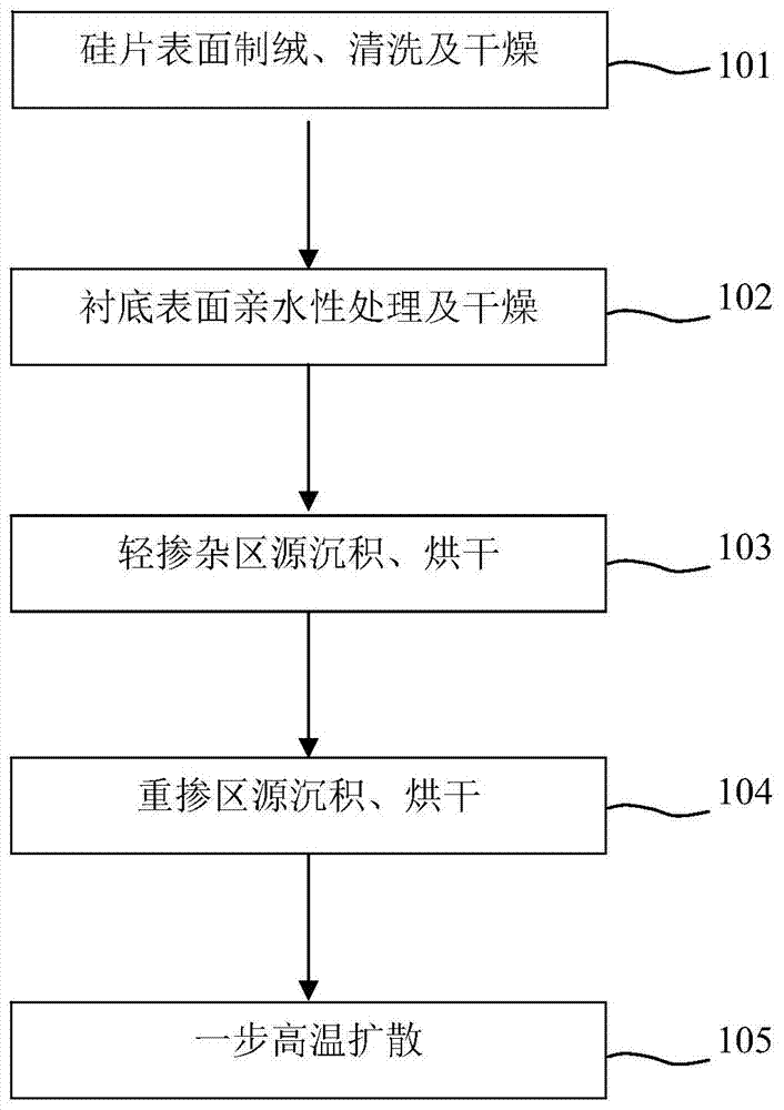
[0034] 1. The substrate is 156×156mm 2 The P-type crystalline silicon wafer (polycrystalline) is subjected to acid etching for texturing, RCA cleaning, and nitrogen blow-drying before use.

[0035] 2. Soak the clean silicon wafer prepared in step 1 in nitric acid solution, carry out wet chemical oxidation on the surface of the silicon wafer to make the surface hydrophilic, and then use nitrogen to dry the silicon wafer for later use, or Tumble dry or tumble dry.

[0036] 3. Prepare a phosphorus salt solution with a concentration of 1.0%wt. as a high-temperature diffusion source in the lightly doped region of the selective emitter structure. After the solution preparation is completed, the prepared phosphorus salt solution is evenly spin-coated and deposited on the surface of the silicon wafer prepared in step 2 by using a glue homogenizer to form a phosphorus salt diffusion source, and then dried for use.

[0037] 4. Use screen printing to deposit silicon ink on the surface ...

Embodiment 2

[0043] 1. The substrate is 156×156mm 2 The P-type crystalline silicon wafer (polycrystalline) is subjected to acid etching for texturing, RCA cleaning, and nitrogen blow-drying before use.

[0044] 2. Soak the clean silicon wafer prepared in step 1 in the RCA-No. 2 solution, perform wet chemical oxidation on the surface of the silicon wafer to make the surface hydrophilic, and then use nitrogen to dry the silicon wafer for later use , can also be tumble dried or tumble dried.

[0045] 3. Prepare a phosphorus salt solution with a concentration of 0.5% wt. as a high-temperature diffusion source in the lightly doped region of the selective emitter structure. After the solution preparation is completed, the prepared phosphorus salt solution is evenly spin-coated and deposited on the surface of the silicon wafer prepared in step 2 by using a glue homogenizer to form a phosphorus salt diffusion source, and then dried for use.

[0046] 4. Use screen printing to evenly spin-coat the...

Embodiment 3

[0052] 1. The substrate is 156×156mm 2 The P-type crystalline silicon wafer (polycrystalline) is subjected to acid etching for texturing, RCA cleaning, and nitrogen blow-drying before use.

[0053] 2. Soak the clean silicon wafer prepared in step 1 in the RCA-No. 3 solution, perform wet chemical oxidation on the surface of the silicon wafer to make the surface hydrophilic, and then use nitrogen to dry the silicon wafer for later use , can also be tumble dried or tumble dried.

[0054] 3. Prepare phosphorus salt aqueous solution with a concentration of 20.0%wt. as a high-temperature diffusion source in the lightly doped region of the selective emitter structure. After the solution preparation is completed, the prepared phosphorus salt source solution is evenly spin-coated and deposited on the surface of the silicon wafer prepared in step 2 by using a glue homogenizer to form a phosphorus salt diffusion source, and then dried for later use.

[0055] 4. Use screen printing to u...


PUM


Abstract

A method for manufacturing a selective emitter structure with low surface concentration and a soft doped zone includes the steps that (1) the surface of a substrate to be prepared is corroded and cleaned, and the surface of the substrate is completely dried after cleaning; (2) the clean substrate prepared in the step (1) is soaked in a solution with high oxidability to carry out wet chemical oxidation on the surface of a silicon wafer, and then the surface of the substrate is completely dried; (3) a microcosmic salt aqueous solution of 0.5-20% is deposited on the surface of the substrate in a spin coating and spraying mode, and then the surface of the substrate is dried; (4) phosphorus ink or silicon ink is deposited on an electrode area on the surface of the substrate coated with a phosphorus source in the step (3) in a screen printing mode, and then the surface of the substrate is dried; (5) the temperature of a diffusion furnace rises, nitrogen is introduced into a diffusion quartz tube, when the temperature reaches 780-890 DEG C, the clean substrate prepared in the step (4) is placed into a constant-temperature area of the diffusion quartz tube, a fire door of the diffusion furnace is sealed, and after the temperature of the diffusion furnace is stable, oxygen is introduced into the diffusion quartz tube; (6) the substrate is taken out and cooled after the diffusion process is over.

Description

technical field [0001] The invention relates to a method for preparing a selective emitter structure of a low surface concentration lightly doped region of a crystalline silicon solar cell. Background technique [0002] Crystalline silicon solar cells still dominate the photovoltaic market, and low cost and high conversion efficiency are still the two major goals of crystalline silicon solar cell technology breakthroughs and production innovations. In the continuous progress of solar cell development and production technology, selective emitter structure solar cells are favored due to their low series resistance and excellent blue light response, which has aroused the interest of many researchers and producers. The characteristic of this selective emitter structure solar cell is that the emitter is composed of a heavily doped emitter region and a lightly doped emitter region, so it is called a selective emitter structure. Among them, the heavily doped emitter is also called...

Claims


Application Information

Patent Timeline
Patent Type & Authority Applications(China)
IPC IPC(8): H01L31/0224H01L31/18
CPCH01L31/022425Y02P70/50
Inventor 汤叶华周春兰陈朋费建明王文静王磊王亚勋王孟夏建汉
Owner INST OF ELECTRICAL ENG CHINESE ACAD OF SCI
Why Eureka
Try Eureka