Nitride semiconductor light-emitting device
A technology of nitride semiconductor and light-emitting device, which is applied in the direction of semiconductor lasers, semiconductor laser optical devices, semiconductor devices, etc., and can solve the problems of characteristic degradation of nitride semiconductor light-emitting elements, and achieve the effect of suppressing characteristic degradation
- Summary
- Abstract
- Description
- Claims
- Application Information
AI Technical Summary
Problems solved by technology
Method used
Image

Examples
Embodiment 1
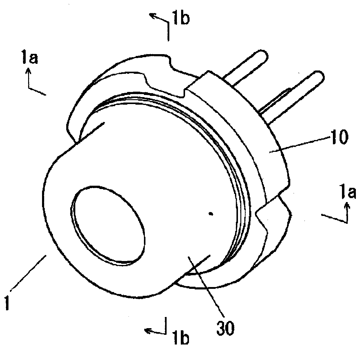
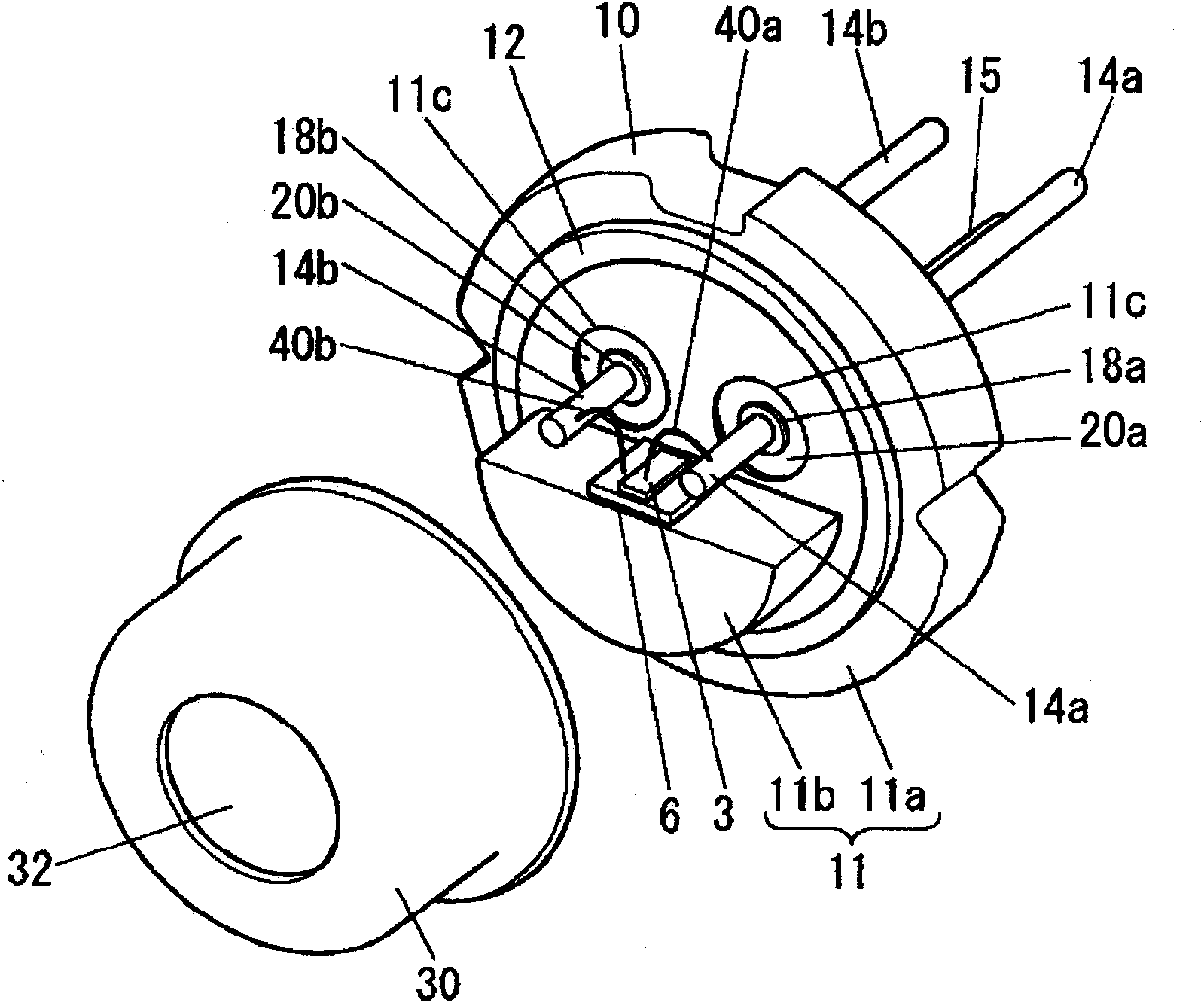
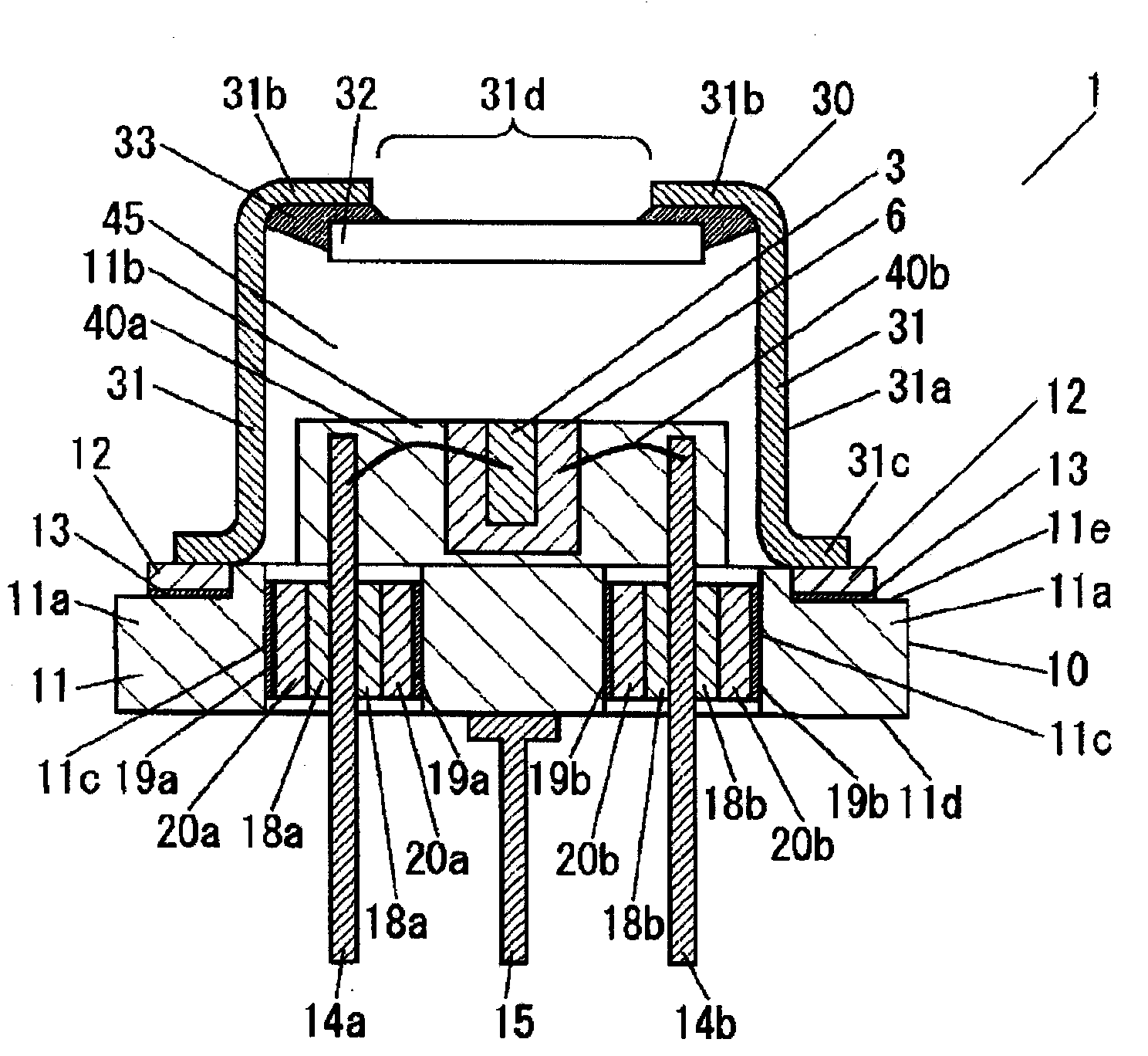
[0065] The nitride semiconductor light emitting device of the first embodiment will be described with reference to FIGS. 1 to 8 . Figure 1A is a perspective view of the nitride semiconductor light-emitting device of this embodiment, Figure 1B It is a perspective view in which the cap 30 is disassembled and detached from the package 10 in order to describe the structure of the nitride semiconductor light emitting device of this embodiment. Figure 2A and Figure 2B It is a schematic cross-sectional view for explaining in detail the structure of the nitride semiconductor light-emitting device of this embodiment, Figure 2A yes Figure 1A The profile of line Ia-Ia, Figure 2B yes Figure 1A Sectional view of the Ib-Ib line. image 3 It is a schematic cross-sectional view of a nitride semiconductor light-emitting element mounted in the nitride semiconductor light-emitting device of this embodiment. Figure 4A and Figure 4B It is a schematic cross-sectional view for expla...
Embodiment 2
[0087] Next, use Figure 9A and Figure 9B The nitride semiconductor light emitting device of the second embodiment will be described. Figure 9A is a cross-sectional view showing the structure of the nitride semiconductor light emitting device of the second embodiment, Figure 9B It is a diagram showing an equivalent circuit of the nitride semiconductor light emitting device of the second embodiment. Components common to those of the first embodiment are denoted by the same reference numerals and descriptions thereof are omitted.
[0088] First, in Figure 9A Among them, there are three nitride semiconductor light-emitting devices 1A, 1B, and 1C of the second embodiment, and a fixing jig 50 for fixing them, a holding jig 51, a collimating lens 53, a lens holder 52, and electrical accessories. Line 58 constitutes.
[0089] In this example, if Figure 9B As shown, the nitride semiconductor light emitting devices 1A, 1B, and 1C are connected in series via electrical wiring...
Embodiment 3
[0091] Next, use Figure 10 The nitride semiconductor light emitting device 201 of the third embodiment will be described. Figure 10 It is a perspective view in which the cap 30 is detached and disassembled from the package 10 of the nitride semiconductor light emitting device of the third embodiment. Components common to those of the first embodiment are denoted by the same reference numerals and descriptions thereof are omitted. The nitride semiconductor light emitting device 201 is greatly different from the nitride semiconductor light emitting device 1 of the first embodiment in the number and shape of buffer members. In the first embodiment, ring-shaped cushioning members were prepared for each of the plurality of introduction needles, but in this embodiment, a common cushioning member is arranged for the plurality of introduction needles. Specifically, the base 11a is provided with a common opening 11c for a plurality of lead pins, and a buffer member 20 having a plur...
PUM
 Abstract
Description
Claims
Application Information
 - R&D
- Intellectual Property
- Life Sciences
- Materials
- Tech Scout
- Unparalleled Data Quality
- Higher Quality Content
- 60% Fewer Hallucinations
Browse by: Latest US Patents, China's latest patents, Technical Efficacy Thesaurus, Application Domain, Technology Topic, Popular Technical Reports.
© 2025 PatSnap. All rights reserved.Legal|Privacy policy|Modern Slavery Act Transparency Statement|Sitemap|About US| Contact US: help@patsnap.com