LED epitaxial wafer and forming method thereof

A technology of LED epitaxial wafers and fractional values, applied in semiconductor devices, electrical components, circuits, etc., can solve the problems of poor crystal quality and difficulty in realization, and achieve flat valence and energy bands, enhanced hole injection, and high energy band peaks Effect

Active Publication Date: 2014-07-09
广东比亚迪节能科技有限公司
View PDF5 Cites 11 Cited by
  • Summary
  • Abstract
  • Description
  • Claims
  • Application Information

AI Technical Summary

Problems solved by technology

However, this structure is difficult to achieve in epitaxy, and at the same time leads to poor crystal quality of P-type

Method used


Image

  • LED epitaxial wafer and forming method thereof
  • LED epitaxial wafer and forming method thereof

Examples


Embodiment Construction

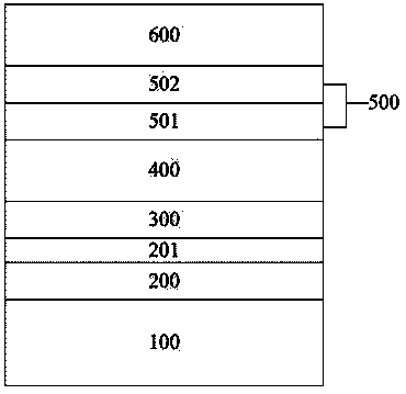
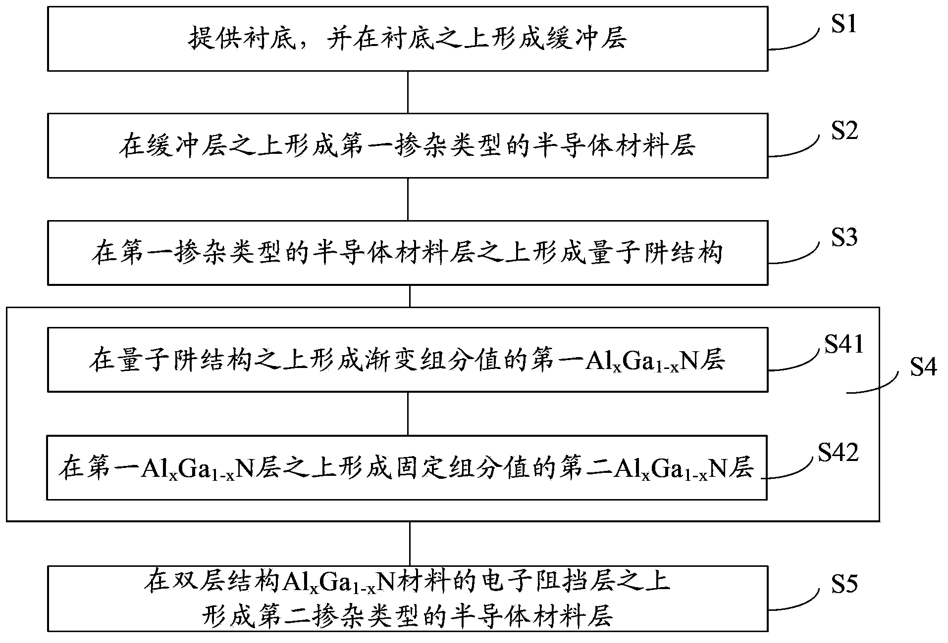
[0025] Embodiments of the present invention are described in detail below, examples of which are shown in the drawings, wherein the same or similar reference numerals designate the same or similar elements or elements having the same or similar functions throughout. The embodiments described below by referring to the figures are exemplary and are intended to explain the present invention and should not be construed as limiting the present invention.

[0026] In describing the present invention, it should be understood that the terms "center", "longitudinal", "transverse", "length", "width", "thickness", "upper", "lower", "front", " Orientation or position indicated by "back", "left", "right", "vertical", "horizontal", "top", "bottom", "inner", "outer", "clockwise", "counterclockwise", etc. The relationship is based on the orientation or positional relationship shown in the drawings, and is only for the convenience of describing the present invention and simplifying the descrip...


PUM


Abstract

The invention proposes an LED epitaxial wafer and a forming method thereof. The forming method comprises a first step of providing a substrate and forming a buffer layer on the substrate; a second step of forming a semiconductor material layer of a first doping type on the buffer layer; a third step of forming a quantum well structure on the semiconductor material layer of the first doping type; a fourth step of forming an electron blocking layer on the quantum well structure; and a fifth step of forming a semiconductor material layer of a second doping type on the electron blocking layer. The fourth step comprises forming a first AlxGa1-xN layer on the quantum well structure, and forming a second AlxGa1-xN layer on the first AlxGa1-xN layer. In the formation of the first AlxGa1-xN layer, a component x of an Al is gradually changed from a first component value to a component value, and the second component value is larger than the first component value. In the formation of the second AlxGa1-xN layer, a component x of an Al is constant. The LED epitaxial wafer and the forming method thereof can improve the internal quantum efficiency of LED chips, promote the light-emitting efficiency of the epitaxial wafer, and are suitable for the needs of high-power epitaxial wafers.

Description

technical field [0001] The invention relates to the technical field of semiconductors, in particular to an LED epitaxial wafer and a forming method thereof. Background technique [0002] With the development of LEDs, GaN-based high-brightness blue light, green light, and ultraviolet LEDs have attracted more and more attention. Semiconductor diodes have been applied to various fields due to their small size, low power consumption, long service life, environmental protection and durability. , For example: blue-green LEDs are widely used in full-color display and lighting, and ultraviolet LEDs are also used in optical detection. The preparation of high-power LED epitaxial wafers has become an inevitable trend of development, but with the increase of luminous power, the problem of efficiency attenuation appears. The problem of attenuation of efficiency is mainly due to carrier overflow and low-efficiency electron injection. and hole transport. The existing method to reduce the...

Claims


Application Information

Patent Timeline
IPC IPC(8): H01L33/04H01L33/32H01L33/14H01L33/00
CPCH01L33/0066H01L33/0075H01L33/06H01L33/145H01L33/32
Inventor 陈飞
Owner 广东比亚迪节能科技有限公司
Why Eureka
Try Eureka