Organic light-emitting diode device used in lighting apparatus

A technology for light-emitting diodes and lighting devices, which is applied to organic semiconductor devices, electrical components, and electrical solid-state devices, etc., can solve problems such as reducing aperture ratio, increasing process cost, and reducing luminous area, thereby improving component yield and simplifying process, the effect of improving luminous efficiency

Inactive Publication Date: 2014-07-09
ULTIMATE IMAGE
View PDF3 Cites 5 Cited by
  • Summary
  • Abstract
  • Description
  • Claims
  • Application Information

AI Technical Summary

Problems solved by technology

However, the existence of the raised structure 106 also reduces the area that can emit light and reduces the aperture ratio (Aperture Ratio)
In addition, the process of concave-convex structure also relatively increases the process cost

Method used


Image

  • Organic light-emitting diode device used in lighting apparatus
  • Organic light-emitting diode device used in lighting apparatus
  • Organic light-emitting diode device used in lighting apparatus

Examples


Embodiment Construction

[0021] In order to further explain the technical means and functions adopted by the present invention to achieve the intended purpose of the invention, the specific embodiments, structures, features and functions of the present invention will be described in detail below in conjunction with the accompanying drawings and preferred embodiments.

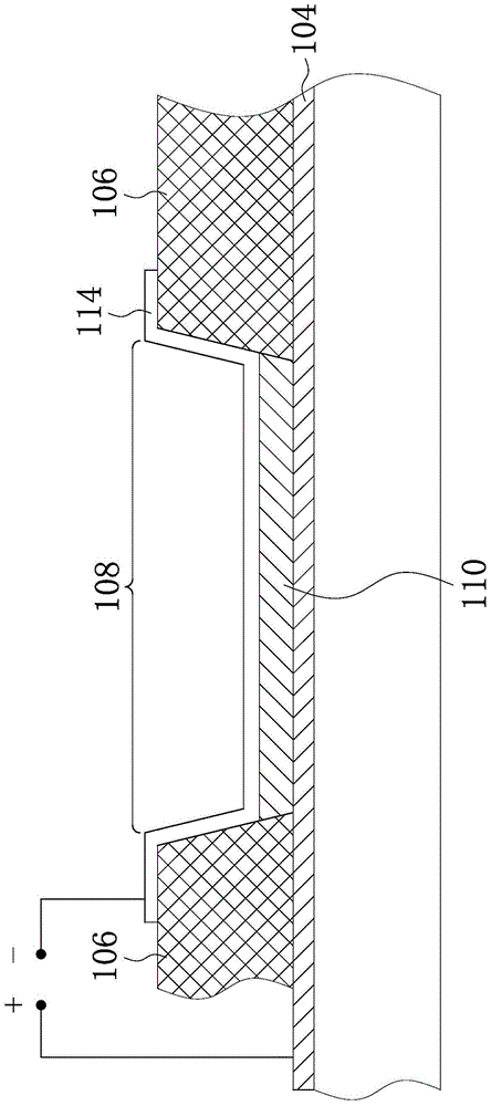
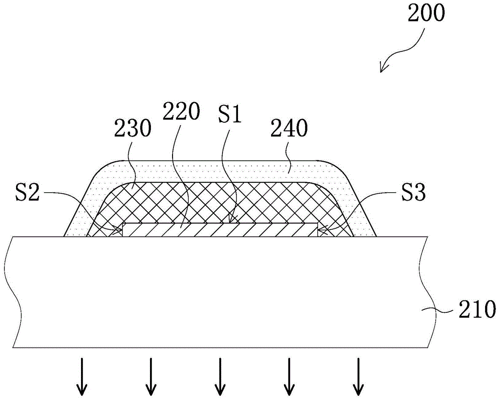
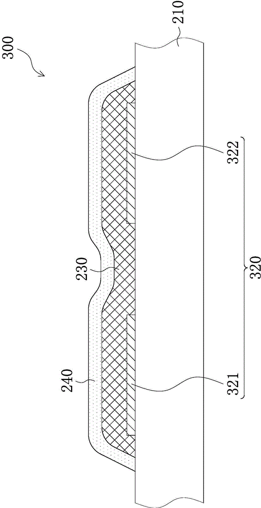
[0022] figure 2 It is a schematic structural diagram of an organic light emitting diode assembly applied to a lighting device according to an embodiment of the present invention. see figure 2 , the organic light emitting diode assembly 200 applied to a lighting device of the present invention includes a substrate 210 , a patterned anode layer 220 , an organic semiconductor layer 230 and a cathode layer 240 . Wherein the patterned anode layer 220 is disposed on the substrate 210 . The organic semiconductor layer 230 covers the upper surface S1 of the patterned anode layer 220 , the sidewalls S2 , S3 and the substrate 210 . The catho...


PUM


Abstract

An organic light-emitting diode device used in a lighting apparatus includes: a substrate; a patterned anode layer disposed on the substrate; an organic semiconductor layer disposed to cover an upper surface and sidewalls of the patterned anode layer and the substrate, wherein a thickness of the organic semiconductor layer is greater than three times of that of the patterned anode layer; and a cathode layer disposed to cover the organic semiconductor layer. According to the invention, a step coverage of the organic semiconductor layer is increased by designing a relative thickness ration of the anode layer and the organic semiconductor layer. In this way, the edge leakage problem can be prevented and a conventional bank structure in an organic light-emitting diode device can be omitted. This improves an element yield rate and increases a light-emitting area of the organic light-emitting diode device.

Description

technical field [0001] The invention relates to an organic light emitting diode component, and in particular to an organic light emitting diode component applied to a lighting device. Background technique [0002] In the existing manufacturing process of Organic Light-Emitting Diode (OLED) components used in displays, most organic polymer layers are used to form a concave-convex structure (generally called a bank structure) to define a specific light-emitting area. To avoid leakage, short circuit and other problems. [0003] Such as figure 1 It can be seen from the schematic cross-sectional view that there is a groove 108 between two adjacent protrusion structures 106 , and the organic semiconductor layer 110 is formed in the groove 108 and disposed between the first transparent electrode 104 and the second electrode 114 . The protruding structure 106 and the organic semiconductor layer 110 separate the first transparent electrode 104 and the second electrode 114 from each...

Claims


Application Information

Patent Timeline
Patent Type & Authority Applications(China)
IPC IPC(8): H01L51/52H01L51/50
CPCH10K50/813H10K71/821
Inventor 宋志峯
Owner ULTIMATE IMAGE
Why Eureka
Try Eureka