Inertial sensor production and wafer level package process based on MEMS (micro-electromechanical system)

A wafer-level packaging, inertial sensor technology, applied in the process of producing decorative surface effects, decorative arts, metal material coating processes, etc., can solve the problems of ASIC design space limitation, MEMS area waste, and high production costs, Achieve the effect of reducing production and testing costs, reducing packaging areas, and improving performance

Inactive Publication Date: 2014-07-16
SENODIA TECH (SHANGHAI) CO LTD
View PDF10 Cites 33 Cited by
  • Summary
  • Abstract
  • Description
  • Claims
  • Application Information

AI Technical Summary

Problems solved by technology

[0008] The purpose of the present invention is to solve the problems of MEMS area waste, limited ASIC design space, high production cost and large chip size in the prior art, and provide a MEMS-based inertial sensor production and wafer-level packaging process, which can The size is reduced to 2-4 square millimeters, and the production cost can be reduced by 30-40% compared with the traditional process

Method used


Image

  • Inertial sensor production and wafer level package process based on MEMS (micro-electromechanical system)
  • Inertial sensor production and wafer level package process based on MEMS (micro-electromechanical system)
  • Inertial sensor production and wafer level package process based on MEMS (micro-electromechanical system)

Examples


Embodiment Construction

[0038] In order to make the technical means, technical features, invention objectives and technical effects realized by the present invention easy to understand, the present invention will be further described below in conjunction with specific illustrations.

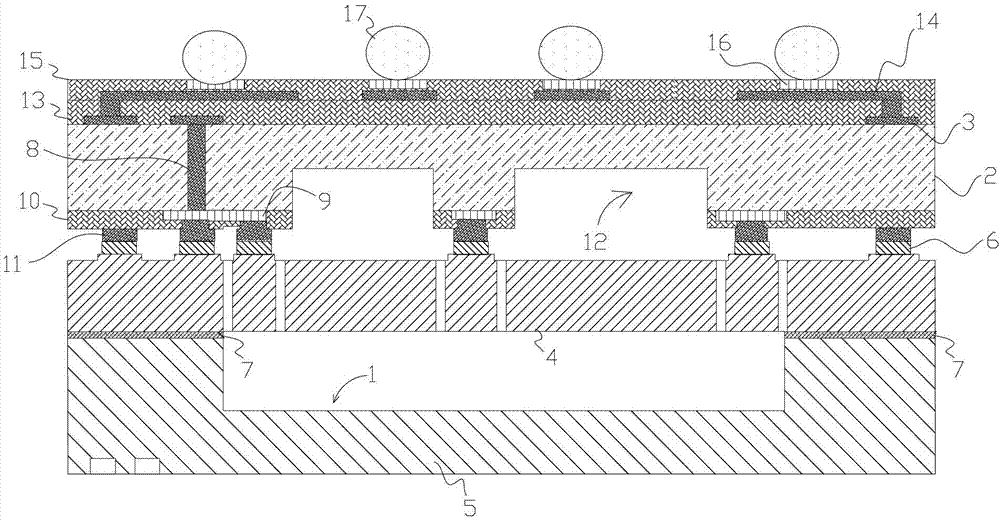
[0039] A production and wafer-level packaging process based on MEMS inertial sensors, see figure 1 , the steps are as follows:

[0040] 1) Engineered silicon-on-insulator formation (E-SOI):

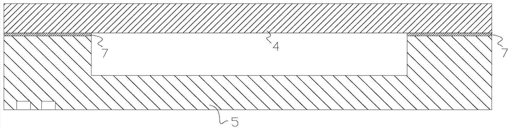
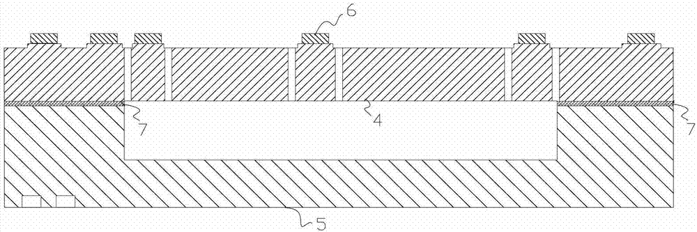
[0041] a. Firstly use silicon to support the wafer (handle wafer) "5", etch the positioning alignment mark (the first photolithography plate) on the back, and then use the plasma process to etch the groove "1" (the second) on the front of the wafer. Photolithography); grow a layer of oxide film "7" by thermal oxidation process; bond with another MEMS wafer (Device wafer) "4" by silicon bonding process;

[0042] b. Grinding to the ideal thickness on the wafer surface of micro-electromechanical devices, such as figure 2 shown;

...


PUM


Abstract

The invention discloses an inertial sensor production and wafer level package process based on an MEMS (micro-electromechanical system). The process includes the steps: 1) forming an E-SOI (engineering-silicon on insulator); 2) performing surface machining on an MEMS wafer; 3) producing an ASIC (application specific integrated circuit) wafer on a standard ASIC foundry; 4) performing metal eutectic bonding for the MEMS wafer and the ASIC wafer; 5) performing WLCSP (wafer level chip size packaging). The area of an ASIC chip is identical with that of an MEMS chip, the effective areas of the MEMS chip and the ASIC chip are sufficiently used, the most effective space is provided for the design of the MEMS chip and the ASIC chip, subsequent package procedures of the chips are omitted by the aid of the wafer level chip size packaging, Flip-Chip of a terminal circuit board is finished directly through a BGA (ball grid array), and the sizes of the chips and production cost are greatly reduced.

Description

technical field [0001] The invention relates to MEMS (micro-electro-mechanical systems) production of inertial sensors, including gyroscopes and accelerators, and in particular to a MEMS (micro-electro-mechanical systems)-based inertial sensor production and wafer-level packaging process. Background technique [0002] In recent years, inertial sensors such as gyroscopes have been more and more widely used in automobiles, smartphones, tablet computers, toy helicopters, and air mice. Gyroscopes and accelerometers based on MEMS are currently mainstream products. Chip design and wafer processing are two key steps in the manufacture of inertial sensors. [0003] However, existing inertial sensors have the following disadvantages on packaged chips and wafers (US Patent No. 7,104,129B2): [0004] (1) Since part of the MEMS (micro-electromechanical system) area must be cut off by a dicing process to expose the metallization area for packaging the leads, part of the MEMS area is was...

Claims


Application Information

Patent Timeline
Patent Type & Authority Applications(China)
IPC IPC(8): B81B7/00B81C1/00
Inventor 韩华邹波
Owner SENODIA TECH (SHANGHAI) CO LTD
Why Eureka
Try Eureka