

Method and device for detecting crystal direction of silicon slice
一种检测方法、硅片的技术,应用在测量装置、半导体/固态器件测试/测量、测试晶体等方向,能够解决不适合全尺寸硅片快速表征、耗时长、成本高等问题
- Summary
- Abstract
- Description
- Claims
- Application Information
AI Technical Summary
Problems solved by technology
Method used
Image

Examples
experiment example 1
[0072] Experimental example 1 uses the method of the present invention to detect silicon wafers with known standard crystal orientations to verify the accuracy of the detection method of the present invention. The steps of Experimental Example 1 and the corresponding experimental data are given below.
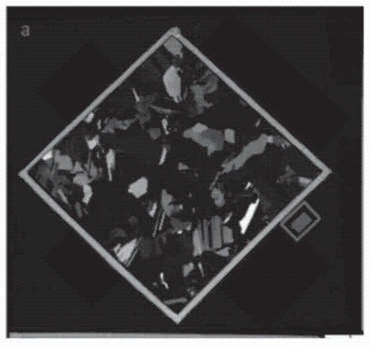
[0073] 1. Put a 1cm×2cm standard commercial oriented small silicon wafer in 2.5% volume concentration KOH solution for 3 minutes;
[0074] 2. If Figure 2a As shown in the box in , place it on a rotating stage and collect the rotation curve of the grain point of interest;
[0075] 3. After obtaining the rotation curve, obtain the angle of its extremum, and solve its (111) surface normal vector according to formula 1, the crystal orientation index vector of the grain at this point can be obtained as , which is consistent with the standard The crystal orientation angle difference is less than 1.5°.
experiment example 2
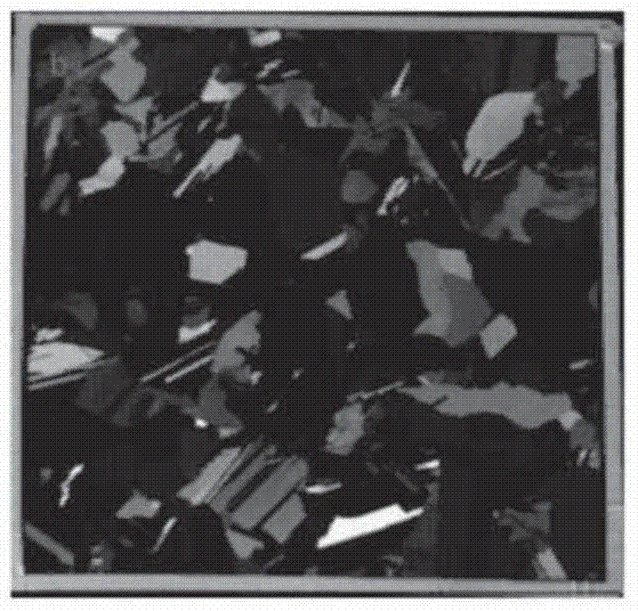
[0077] Experimental example 2 uses the method of the present invention to detect the entire surface of a polycrystalline silicon wafer, and determines the crystal orientation of each crystal grain, thereby knowing the distribution of crystal orientations on the entire polycrystalline silicon wafer surface.
[0078] Experimental example 2 and corresponding experimental data are given below.
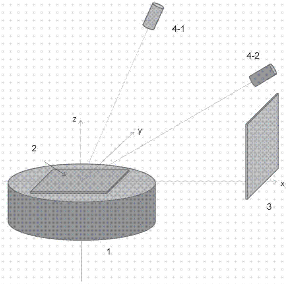
[0079] 1. Put the silicon carbide mortar cut polysilicon wafer into the KOH solution with a volume concentration of 2.5% and corrode it for 3 minutes;
[0080] 2. Put the etched silicon wafer on figure 1 Optical measurement is carried out on the device, in which the step angle of the rotary table is 0.1;
[0081] 3. Obtain the reflection spectrum of all crystal grains by digital image processing method;
[0082] 4. Calculate the crystal orientation of the reflectance spectrum according to formula 1 to obtain the precise crystal orientation of all crystal grains. For the convenience of ...
PUM
 Abstract
Description
Claims
Application Information