PID resistance crystalline silicon battery and preparation method thereof

A technology of crystalline silicon cells and electrodes, which is applied in circuits, electrical components, semiconductor devices, etc., can solve the problems of reduced photocurrent, high extinction coefficient of silicon nitride, and reduced cell efficiency. The method is simple, good resistance to PID, and low cost. cheap effect

Inactive Publication Date: 2014-07-16
SUZHOU TALESUN SOLAR TECH CO LTD
View PDF4 Cites 26 Cited by
  • Summary
  • Abstract
  • Description
  • Claims
  • Application Information

AI Technical Summary

Problems solved by technology

[0006] Generally, the density of the silicon nitride anti-reflection film is increased on the battery side, that is, the method of increasing the refractive index is used to block the erosion of positive ions on the PN junction, thereby reducing the influence of the PID effect, but this method requires silicon nitride The refractive index of the silicon nitride is increased to about 2.2. The extinction coefficient of silicon nitride with such a high refractive index will be very high. The silicon nitride film itself will absorb more light, and the light incident on the substrate will decrease, resulting in a decrease in the photogenerated current, resulting in drop in battery efficiency

Method used


Image

  • PID resistance crystalline silicon battery and preparation method thereof

Examples


Embodiment Construction

[0028] The present invention will be described in detail below with reference to the accompanying drawings and in combination with embodiments.

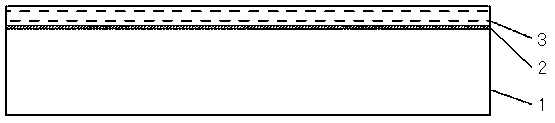
[0029] refer to figure 1 As shown, an anti-PID crystalline silicon battery includes a silicon dioxide layer 2 and a silicon nitride antireflection layer 3 covering a silicon substrate 1 in sequence. The silicon dioxide layer 2 has a thickness of 1-5 nm. The antireflection layer 3 of the silicon nitride layer has a thickness of 70-85nm.

[0030] A method for preparing an anti-PID crystalline silicon battery. After the silicon substrate 1 is cleaned, textured, diffused, dephosphorized silicon glass, and edge etched in the conventional process steps, the silicon substrate 1 is placed under a low-pressure ultraviolet mercury lamp. Continuous irradiation for 30 minutes.

[0031] The low-pressure ultraviolet mercury lamp can emit two kinds of ultraviolet light of different wavelengths at the same time, and integrates the ozone generatin...


PUM

PropertyMeasurementUnit
thicknessaaaaaaaaaa
thicknessaaaaaaaaaa

Abstract

The invention discloses a PID resistance crystalline silicon battery. The PID resistance crystalline silicon battery comprises a silicon dioxide layer and a silicon nitride antireflecting layer which sequentially cover a silicon substrate. A preparation method of the PID resistance crystalline silicon battery comprises the following steps that cleaning, texturing, diffusion, phosphorosilicate glass removing and edge etching are conducted on the silicon substrate; ozone is generated on the surface of the silicon substrate through an ozone generation device, then the silicon substrate is placed under a UV lamp to be irradiated, and a layer of silicon oxide is grown; PECVD equipment is used for growing the silicon nitride antireflecting layer on the silicon oxide, and then printing and sintering of electrodes on a front face and a back face are achieved. According to the PID resistance crystalline silicon battery, the structure of an antireflecting layer of the battery is mainly improved, the compact silicon dioxide layer is prepared between traditional single-layer or multi-layer silicon nitride and the crystalline silicon substrate by using the UV lamp for irradiating, the silicon dioxide layer can prevent erosion of positive ions to PN junctions, and therefore the influence of a PID effect is reduced.

Description

[0001] technical field [0002] The invention relates to the production field of crystalline silicon solar cells, in particular to an anti-PID crystalline silicon cell and a preparation method thereof. Background technique [0003] PID (Potential-Induced Decay) phenomenon refers to the phenomenon that the output power of solar crystalline silicon modules attenuates when they work in a humid and hot environment and under high voltage for a long time. It is generally believed that the sodium ions in the glass are precipitated in a hot and humid environment, and through the circuit formed by the crystalline silicon battery and packaging materials to the frame of the module under high voltage, the PN junction of the battery is eroded, which is the main cause of the PID phenomenon. In recent years, PID has become one of the important factors for foreign buyers to complain about the quality of domestic modules. In severe cases, it can cause the power of a module to attenuate by mo...

Claims


Application Information

Patent Timeline
Patent Type & Authority Applications(China)
IPC IPC(8): H01L31/0216H01L31/0352H01L31/18
CPCH01L31/02168Y02P70/50
Inventor 陆俊宇
Owner SUZHOU TALESUN SOLAR TECH CO LTD
Why Eureka
Try Eureka