MEMS (Micro-Electromechanical System) sensor encapsulation structure and encapsulation method thereof

A packaging structure and packaging method technology, applied in the direction of microstructure devices, manufacturing microstructure devices, microstructure technology, etc., can solve problems such as difficult wiring, achieve strong scalability, compact overall device structure, and easy wiring layout Effect

Active Publication Date: 2014-07-30
INST OF GEOLOGY & GEOPHYSICS CHINESE ACAD OF SCI
View PDF9 Cites 30 Cited by
  • Summary
  • Abstract
  • Description
  • Claims
  • Application Information

AI Technical Summary

Problems solved by technology

[0004] The purpose of the present invention is to address the deficiencies of the prior art, to provide a base that can be easily expanded into a multi-level structure according to needs, and the wires can be arranged in layers in the base, which can solve the problem of difficult wiring; provide A packaging structure with low packaging stress and good airtightness is provided, and the packaging method of the packaging structure is provided at the same time, which effectively improves production efficiency and reduces costs, and is suitable for harsh environments such as high temperature and high humidity.

Method used


Image

  • MEMS (Micro-Electromechanical System) sensor encapsulation structure and encapsulation method thereof
  • MEMS (Micro-Electromechanical System) sensor encapsulation structure and encapsulation method thereof
  • MEMS (Micro-Electromechanical System) sensor encapsulation structure and encapsulation method thereof

Examples


Embodiment Construction

[0037] The present invention will be described in detail below in conjunction with the embodiments and the accompanying drawings. It should be noted that the described embodiments are only intended to facilitate the understanding of the present invention, rather than limiting it in any way.

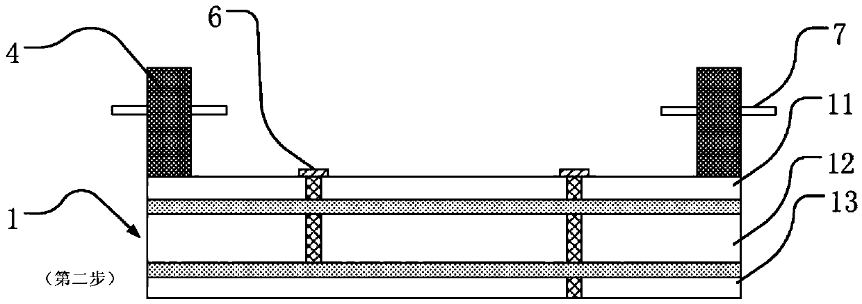
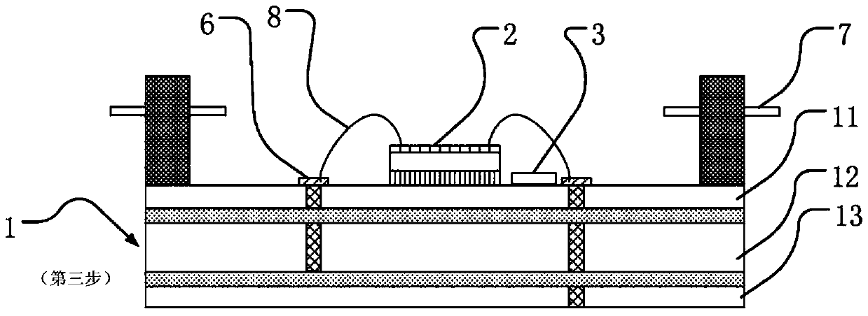
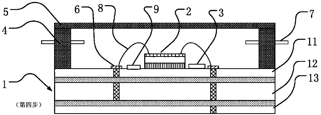
[0038] Based on the use environment of the product of the present invention, long-term outdoor operation is required, which brings severe challenges to the airtightness of the accelerometer packaging process, harsh environments such as high temperature and high humidity, and packaging stress.

[0039] refer to Figure 1 to Figure 8 , the present invention provides a MEMS sensor packaging structure, which is used to package MEMS sensors, the packaging structure comprising:

[0040] A ceramic base 1, the top layer 11 and the bottom layer 13 of the ceramic base 1 are respectively provided with a plurality of metal pads 6; the metal pads 6 of the top layer 11 of the ceramic base are connected...


PUM

PropertyMeasurementUnit
thicknessaaaaaaaaaa

Abstract

The invention relates to an MEMS sensor encapsulation structure and an encapsulation method thereof, which are used for encapsulating an MEMS sensor. The MEMS sensor encapsulation structure is characterized by comprising a ceramic base, a side wall and a top cap, wherein a plurality of metal bonding pads are respectively arranged on a top layer and a bottom layer of the ceramic base; the metal bonding pads on the top layer of the ceramic base are connected with leads of the MEMS sensor; the MEMS sensor is arranged on the ceramic base; the metal bonding pads on the bottom layer of the ceramic base are connected with an external circuit; the ceramic base adopts one-layer or multi-layer perpendicularly interconnected structure; the side wall and the top cap are both made of kovar alloy. According to the invention, the ceramic base of which coefficient of thermal expansion is approximate to that of the MEMS sensor material is selected as the encapsulation material, in order to reduce influence of the base expansion stress to the MEMS sensor; meanwhile, the ceramic base can be utilized to realize one-layer perpendicular interconnection or multi-layer perpendicular interconnection; the system-level integration between the MEMS sensor and the peripheral circuit can be realized within a small area; high-density system-level encapsulation can be realized; the encapsulation flexibility and the expansibility of the MEMS sensor can be realized.

Description

technical field [0001] The invention relates to the field of component packaging structure and packaging method thereof, in particular to a MEMS (micro-electromechanical system) sensor packaging structure and packaging method; the invention also relates to a MEMS accelerometer utilizing the packaging structure and method. Background technique [0002] Multi-chip module refers to the integration of multiple bare or / and packaged integrated circuit chips and single or multiple passive components, such as resistors, capacitors, inductors, etc., into a package base to form a system or functional module a technique. At present, electronic component chips are developing in a more and more complex direction, and traditional IC integrated device packaging and metal tube packaging will bring difficulties. For example, for MEMS sensors (such as MEMS accelerometers and MEMS gyroscopes), in order to improve their performance, it is often necessary to increase the thickness of the movabl...

Claims


Application Information

Patent Timeline
Patent Type & Authority Applications(China)
IPC IPC(8): B81B7/00B81C1/00G01P15/125
Inventor 薛旭郭士超
Owner INST OF GEOLOGY & GEOPHYSICS CHINESE ACAD OF SCI
Why Eureka
Try Eureka