Preparation method of semi-polar m-plane GaN base semiconductor device containing SiNx insertion layer

A semi-polar and intercalated layer technology, applied in the field of microelectronics, can solve the problems of high cost, excessive, and affecting the quality of GaN, and achieve the effects of quality improvement, time and material cost reduction, and convenient and simple experimental process

Inactive Publication Date: 2014-07-30
XIDIAN UNIV
View PDF0 Cites 15 Cited by
  • Summary
  • Abstract
  • Description
  • Claims
  • Application Information

AI Technical Summary

Problems solved by technology

However, this method requires multiple etching photolithography processes, resulting in high cost and complex process
In sit

Method used


Image

  • Preparation method of semi-polar m-plane GaN base semiconductor device containing SiNx insertion layer
  • Preparation method of semi-polar m-plane GaN base semiconductor device containing SiNx insertion layer
  • Preparation method of semi-polar m-plane GaN base semiconductor device containing SiNx insertion layer

Examples


Embodiment 1

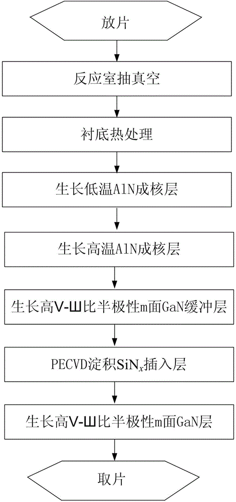
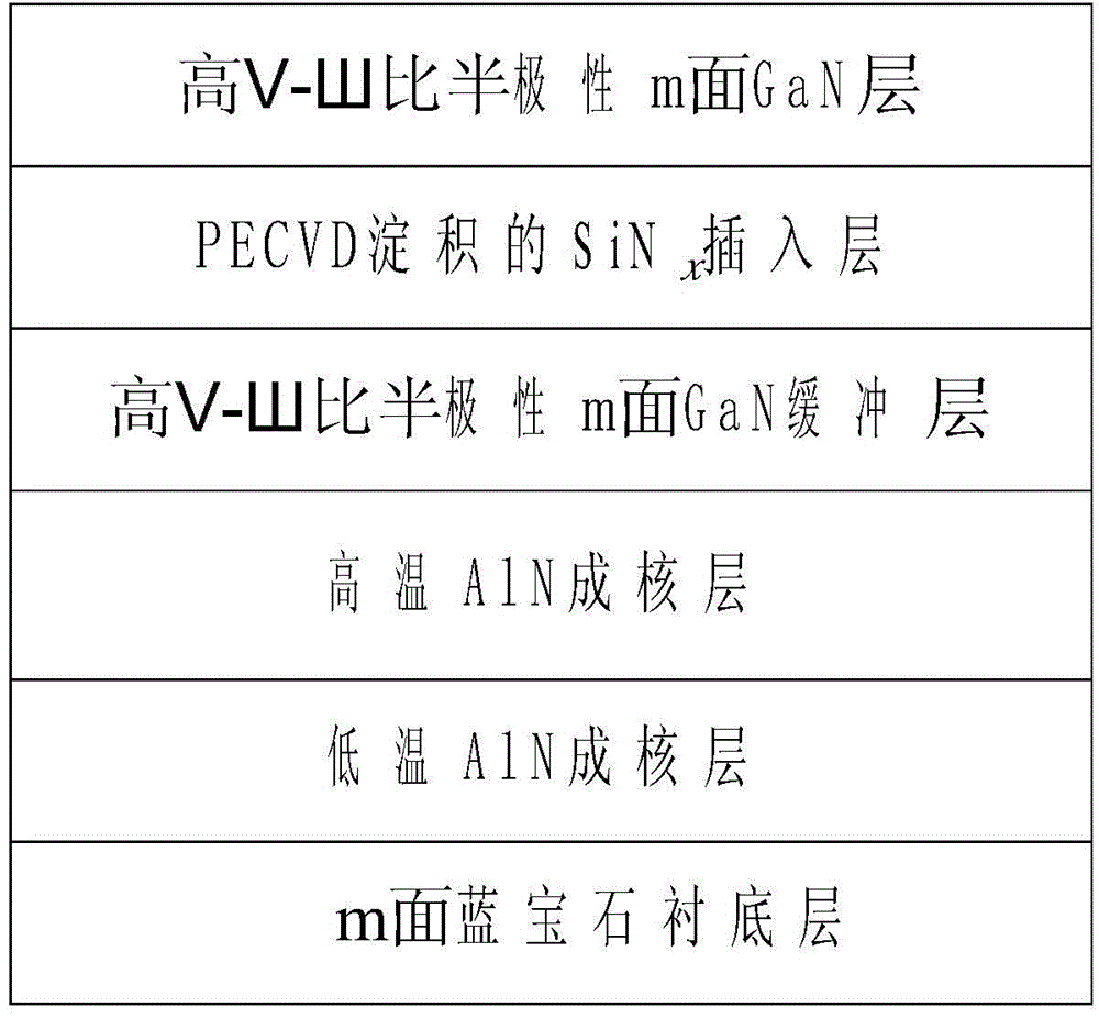
[0024] The realization steps of the present invention are as follows:

[0025] Step 1, performing heat treatment on the substrate.

[0026] Place the m-plane sapphire substrate in a metal-organic chemical vapor deposition (MOCVD) reaction chamber, and pass a mixed gas of hydrogen and ammonia into the reaction chamber to heat-treat the substrate. The vacuum degree of the reaction chamber is less than 2 ×10 -2 Torr, the substrate heating temperature is 900° C., the time is 5 minutes, and the reaction chamber pressure is 20 Torr after the mixed gas is introduced, and the substrate is heat-treated.

[0027] Step 2, growing a low-temperature AlN nucleation layer at a temperature of 600°C.

[0028] Lower the temperature of the substrate after heat treatment to 600oC, feed the aluminum source (trimethylaluminum) with a flow rate of 5 μmol / min, hydrogen gas with a flow rate of 1200 sccm and ammonia gas with a flow rate of 1000 sccm into the reaction chamber, and keep the pressure at...

Embodiment 2

[0041] The realization steps of the present invention are as follows:

[0042] Step A, performing heat treatment on the substrate.

[0043] Put the m-plane sapphire substrate in the metal organic chemical vapor deposition MOCVD reaction chamber, and pass the mixed gas of hydrogen and ammonia into the reaction chamber to heat-treat the substrate. The vacuum degree of the reaction chamber is less than 2×10 -2 Torr, the substrate heating temperature is 1020° C., the time is 8 minutes, and the reaction chamber pressure is 40 Torr, and the substrate is heat-treated.

[0044] Step B, growing a low temperature AlN nucleation layer with a temperature of 620°C.

[0045] Lower the temperature of the substrate after the heat treatment to 620°C, feed the aluminum source with a flow rate of 13 μmol / min, hydrogen gas with a flow rate of 1200 sccm and ammonia gas with a flow rate of 3000 sccm into the reaction chamber, and grow to a thickness of 20 nm under the condition of maintaining a pr...

Embodiment 3

[0057] The realization steps of the present invention are as follows:

[0058] In step one, heat treatment is performed on the substrate.

[0059] Put the m-plane sapphire substrate in the metal organic chemical vapor deposition MOCVD reaction chamber, and pass the mixed gas of hydrogen and ammonia into the reaction chamber to heat-treat the substrate. The vacuum degree of the reaction chamber is less than 2×10 -2 Torr, the substrate heating temperature is 1080° C., the time is 10 minutes, and the reaction chamber pressure is 760 Torr, and the substrate is heat-treated.

[0060] Step 2, growing a low-temperature AlN nucleation layer at a temperature of 800°C.

[0061] Lower the temperature of the heat-treated substrate to 800°C, feed the aluminum source with a flow rate of 100 μmol / min, hydrogen gas with a flow rate of 1200 sccm, and ammonia gas with a flow rate of 10000 sccm into the reaction chamber, and grow to a thickness of 40 nm under the condition of maintaining a pres...


PUM

PropertyMeasurementUnit
Thicknessaaaaaaaaaa
Thicknessaaaaaaaaaa
Thicknessaaaaaaaaaa

Abstract

The present invention discloses a preparation method of a semi-polar m-plane GaN base semiconductor device containing a SiNx insertion layer. The preparation method mainly comprises: (1)placing a m-plane sapphire substrate in a MOCVD reaction chamber, introducing hydrogen gas and ammonia gas mixed gas, and carrying out a heat treatment on the substrate; (2) growing a low temperature AlN nucleation layer with a thickness of 15-40 nm on the substrate; (3) growing a high temperature AlN nucleation layer with a thickness of 90-150 nm on the low temperature nucleation layer; (4) growing a GaN buffer layer with a thickness of 1000-2500 nm on the AlN nucleation layer; (5) depositing a SiNx insertion layer on the m-plane GaN buffer lay and in the PECVD; and (6) growing a GaN epitaxial layer with a thickness of 4000-6000 nm on the SiNx insertion layer. The m-plane GaN film has the advantage of low defect, and can be used for production of the semi-polar m-plane GaN light-emitting diodes.

Description

technical field [0001] The invention belongs to the technical field of microelectronics, and relates to a method for growing semiconductor materials, in particular to a SiN based on PECVD deposition. x The metal organic compound chemical vapor deposition MOVCD method of the semi-polar m-plane GaN semiconductor material of the insertion layer can be used to manufacture semi-polar m-plane GaN-based semiconductor devices. technical background [0002] Semiconductor materials composed of Group III elements and Group V elements, that is, Group III-V compound semiconductor materials, such as GaN, GaAs, InP-based semiconductor materials, often have large gaps in their band gaps, so people usually use these III - Group V compound semiconductor materials form various heterostructures for various electronic devices. Due to the very strong spontaneous polarization and piezoelectric polarization on the c-plane GaN, there is a two-dimensional electron gas 2DEG with high density and high...

Claims


Application Information

Patent Timeline
IPC IPC(8): C23C16/34C23C16/44H01L21/02H01L21/205
Inventor 许晟瑞曹荣涛张进成郝跃张帅郭求是范晓萌卢知伯
Owner XIDIAN UNIV
Why Eureka
Try Eureka