A Microstrip Dielectric Phase Shifter Can Suppress High Frequency Radiation Loss

A radiation loss, microstrip line technology, used in antennas, waveguide devices, electrical components, etc., can solve the problems of large loss, reduce energy transmission rate, large loss, etc., achieve simple production, suppress high-frequency radiation loss, reduce Effects of Radiation Loss

Active Publication Date: 2017-03-22
NAT UNIV OF DEFENSE TECH
View PDF6 Cites 0 Cited by
  • Summary
  • Abstract
  • Description
  • Claims
  • Application Information

AI Technical Summary

Problems solved by technology

[0004] Microstrip linear dielectric phase shifters have relatively large losses in high-frequency applications, including insertion loss, dielectric loss, return loss, conductor loss, radiation loss, etc., which greatly reduce the energy transmission rate, and the higher the frequency, The greater the loss

Method used


Image

  • A Microstrip Dielectric Phase Shifter Can Suppress High Frequency Radiation Loss
  • A Microstrip Dielectric Phase Shifter Can Suppress High Frequency Radiation Loss
  • A Microstrip Dielectric Phase Shifter Can Suppress High Frequency Radiation Loss

Examples


Embodiment 1

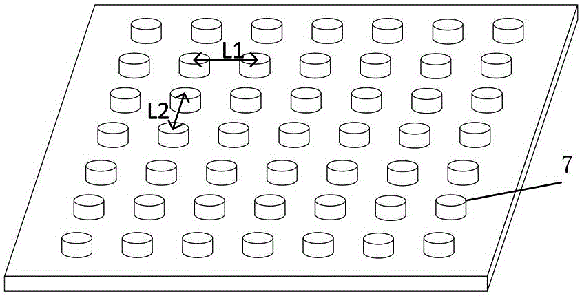
[0029] Embodiment 1: as Figure 4 As shown, holes 5 are drilled on the reference ground electrode layer 2 , and the distance between adjacent holes 5 is less than or equal to λ / 2; the height of the photonic crystal structure 7 is the thickness of the reference ground electrode layer 2 . The hole 5 is cylindrical, and there is no filler in the hole 5 . In other examples, some materials other than metal electrodes can also be filled in the cylindrical hole 5 .

[0030] When making, use the order from bottom to top to make. First, a layer of metal is made on the substrate 1 as the reference ground electrode layer 2; then, through a series of semiconductor processes such as glue coating, photolithography, and corrosion, periodic holes 5 are etched on the reference ground electrode layer 2; then , make a dielectric thin film layer 3 on the reference ground electrode layer 2; finally make a layer of metal on the dielectric thin film layer 3, and etch out the shape of the required t...

Embodiment 2

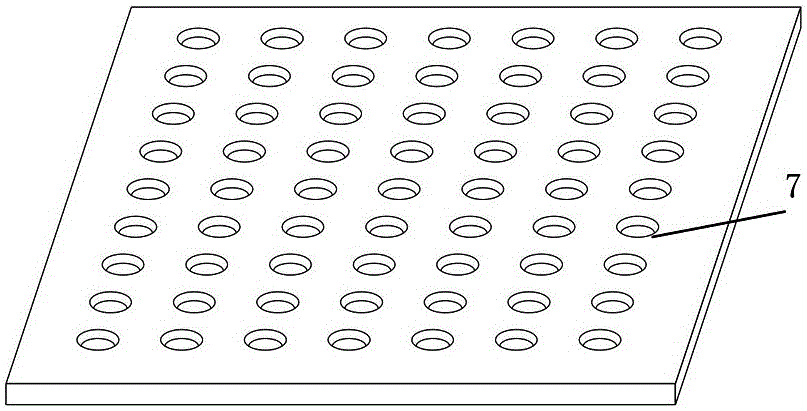
[0031] Embodiment 2: as Figure 5 As shown, cylindrical holes 5 are drilled on the dielectric film layer 3 , the spacing between adjacent holes 5 is less than or equal to λ / 2, and the height of the photonic crystal structure 7 is the thickness of the dielectric film layer 3 . The cylindrical hole 5 may have no filler, and there is no filler in the hole 5 . In other examples, it is also possible to choose to fill the cylindrical hole 5 with some material different from the metal electrode.

[0032] When making, use the order from bottom to top to make. First, make a layer of metal on the substrate 1 as the reference ground electrode layer 2; then make a dielectric thin film layer 3 on the reference ground electrode layer 2; Periodic holes 5 are etched on the thin film layer 3; finally, a layer of metal is formed on the dielectric thin film layer 3, and the shape of the required transmission line layer 4 is etched through a series of semiconductor processes such as glue coating...

Embodiment 3

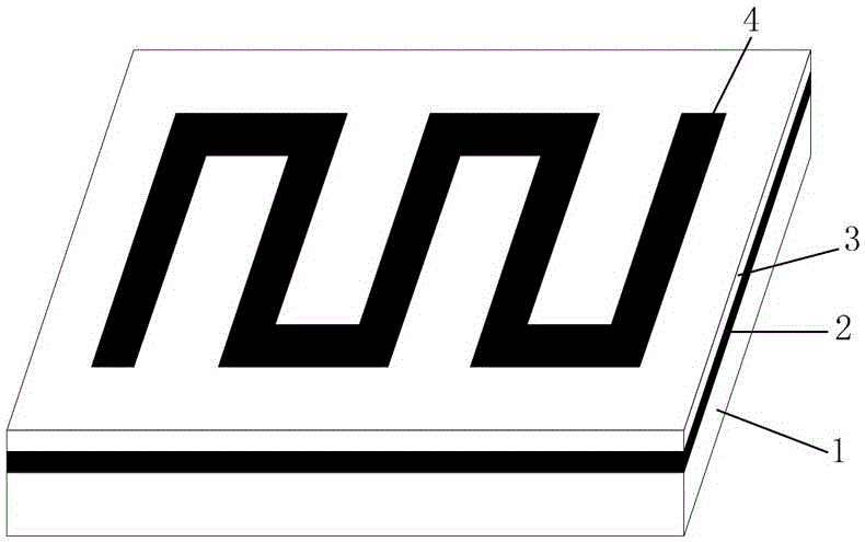
[0033] Embodiment 3: as Figure 6 As shown, cylindrical metal pillars 6 are made in the blank space around the transmission line layer 4 , the distance between adjacent pillars 6 is less than or equal to λ / 2, and the height of the pillars 6 is the same as the thickness of the transmission line layer 4 .

[0034] When making, use the order from bottom to top to make. First, make a layer of metal on the substrate 1 as the reference ground electrode layer 2; then make a dielectric film layer 3 on the reference ground electrode layer 2; then make a layer of metal on the dielectric film layer 3; finally, in the transmission line layer On the metal layer 4, through a series of semiconductor processes such as gluing, photolithography, and corrosion, the shape of the transmission line layer 4 required and the pillars 6 forming the photonic crystal structure 7 are etched out.

[0035] It can be understood that, in addition to the single-layer photonic crystal structure 7 in the above ...


PUM


Abstract

The invention discloses a microstrip line dielectric phase shifter capable of restraining high-frequency radiation loss. The microstrip line dielectric phase shifter comprises a substrate, a reference ground electrode layer, a dielectric film layer and a transmission line layer which are sequentially distributed in a stacked mode , wherein at least one of the substrate, the reference ground electrode layer, the dielectric film layer and the transmission line layer is provided with a photonic crystal structure. The microstrip line dielectric phase shifter has the advantages of being simple and compact in structure, easy and convenient to manufacture, and capable of restraining high-frequency radiation of devices, reducing high-frequency loss of the device, and the like.

Description

technical field [0001] The invention mainly relates to the field of microwave radio frequency circuits, in particular to a microstrip dielectric phase shifter capable of suppressing high-frequency radiation loss. Background technique [0002] Electronically scanned antenna arrays have important applications in communication systems, phased array radar, defect detection and other fields. The phase shifter is the core component of the electronically scanned antenna array, which determines the performance and cost of the system. Fast phase shifting speed, high phase shifting accuracy, small insertion loss, large power capacity, small size, light weight, low cost, and high reliability are the development needs of millimeter wave phase shifters. There are more and more ways to implement microwave phase shifters, such as semiconductor diode phase shifters, gallium arsenide transistor switching phase shifters, ferrite phase shifters, and dielectric phase shifters. Among these pha...

Claims


Application Information

Patent Timeline
Patent Type & Authority Patents(China)
IPC IPC(8): H01P1/18H01Q3/34
Inventor 陈书明张金英宁希池雅庆梁斌
Owner NAT UNIV OF DEFENSE TECH
Why Eureka
Try Eureka