
A kind of quasi-single crystal silicon ingot growth method

A growth method and technology of quasi-single crystal silicon, applied in the directions of single crystal growth, single crystal growth, crystal growth, etc., can solve the problems of low cell efficiency, no obvious advantages, and reduced utilization rate of quasi-single crystal ingots, etc. Achieve the effect of low dislocation rate, no crucible contact pollution, and high single crystal rate

Active Publication Date: 2017-01-04
江苏盎华光伏工程技术研究中心有限公司
View PDF4 Cites 0 Cited by
  • Summary
  • Abstract
  • Description
  • Claims
  • Application Information

AI Technical Summary

Problems solved by technology

The quasi-single crystal grown by this method has a single crystal rate of only about 60%. There are a large number of high dislocation areas where polycrystals and single crystals coexist in the silicon ingot area in contact with the crucible wall. crystalline cells are still relatively low, resulting in lower utilization of quasi-monocrystalline ingots
The existing quasi-monocrystalline silicon ingot technology does not show obvious advantages compared with polycrystalline silicon ingot casting

Method used


Image

  • A kind of quasi-single crystal silicon ingot growth method
  • A kind of quasi-single crystal silicon ingot growth method

Examples


Embodiment Construction

[0020] The present invention will be further described below in conjunction with the accompanying drawings and embodiments.

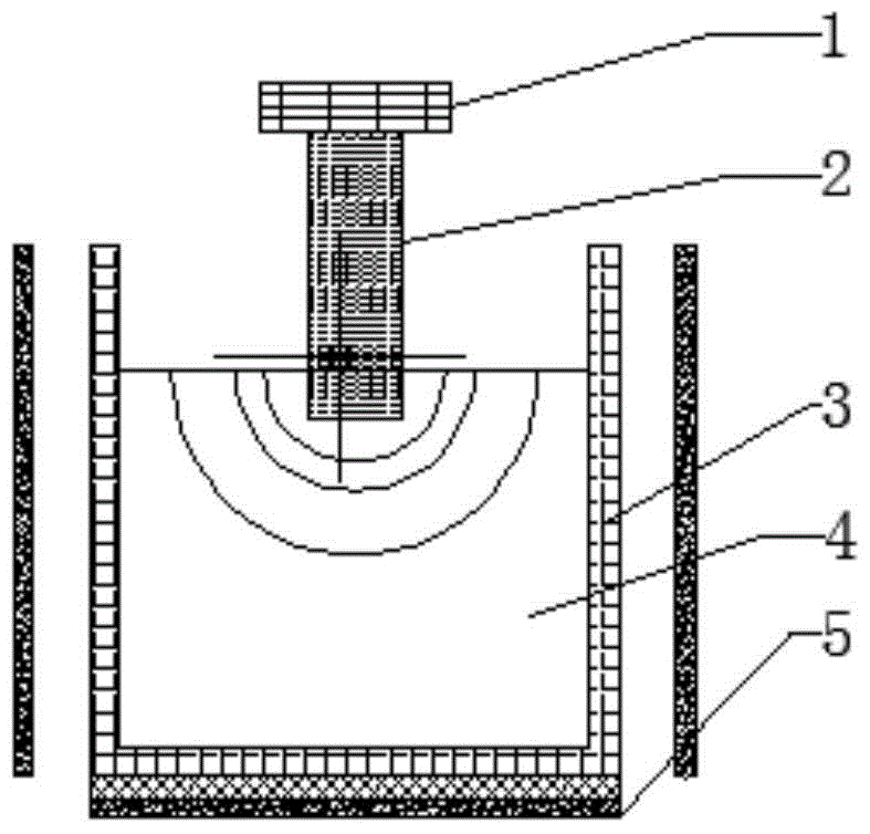
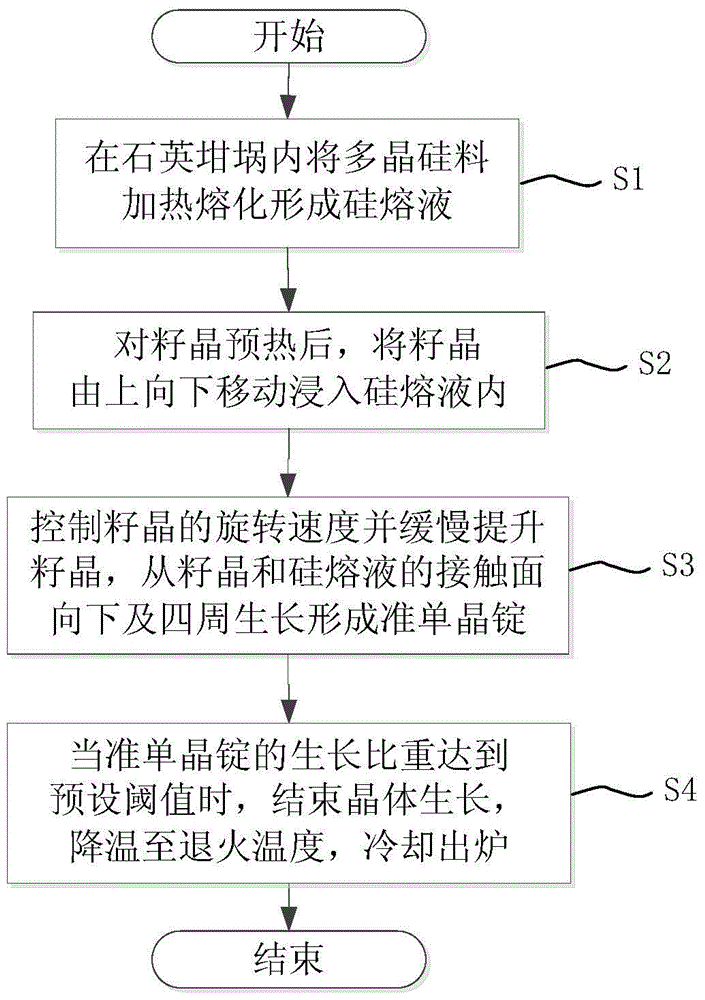
[0021] figure 1 A schematic structural view of the quasi-single crystal silicon ingot furnace used in the present invention; figure 2 It is a schematic diagram of the growth control process of the quasi-single crystal silicon ingot of the present invention.

[0022] See figure 1 and figure 2 , the quasi-single crystal silicon ingot growth method provided by the present invention, the seed crystal 2 with the cooler 1 is immersed in the silicon melt from the top, and the quasi-single crystal growth method is carried out. The heat is mainly taken away by the seed crystal 2 with the cooler 1 and the inert gas flow; the seed crystal with the cooler is connected with a power mechanism, which can realize the rotation and lifting of the seed crystal. The polysilicon material is put into a quartz crucible 3 with a silicon nitride coating for melting, and i...


PUM

PropertyMeasurementUnit
diameteraaaaaaaaaa
lengthaaaaaaaaaa
crystal orientationaaaaaaaaaa

Abstract

The invention discloses a growing method of a pseudo-monocrystal silicon ingot. The growing method comprises the following steps: a) heating a polycrystalline silicon material in a quartz crucible to be melted to form a silicon melt; b) after pre-heating seeds, movably immersing the seeds into the silicon melt from top to bottom; c) controlling the rotating speed of the seeds and slowly lifting the seeds and growing from the contact face of the seeds and the silicon melt downward and all around to form the pseudo-monocrystal silicon ingot; and d) when the growing proportion of the pseudo-monocrystal silicon ingot reaches the predetermined threshold valve, finishing growth of crystals, cooling to annealing temperature and cooling and discharging. According to the growing method of the pseudo-monocrystal silicon ingot provided by the invention, the seeds are immersed into the silicon melt from top to bottom and the seeds are control to rotate and lifted upward, so that liquid silicon exists between the pseudo-monocrystal silicon ingot and the wall of the quartz crucible during growth to effectively avoid direct contact of the pseudo-monocrystal silicon ingot and the quartz crucible, thereby having the advantages of high monocrystal rate and low dislocation rate. No crucible contact pollution is generated and the edge layer needs not to be removed.

Description

technical field [0001] The invention relates to a method for preparing silicon ingots for solar cells, in particular to a method for growing quasi-single crystal silicon ingots. Background technique [0002] With the continuous development of the solar power generation industry, silicon solar cells have become mainstream products in the civilian market due to their low price and relatively mature technology. Solar cells made of monocrystalline silicon have high efficiency, but generally monocrystalline silicon is made by the Czochralski method, and the cost is high, while polycrystalline silicon is cast in ingots by heat exchange, and the cost is low, but the battery made of it The efficiency is relatively low. [0003] It can be seen that the development of quasi-single crystal growth using polysilicon ingots has become a new technology. Generally, the quasi-single crystal ingot adopts the method of laying the seed crystal at the bottom, and the ingot casting starts in th...

Claims


Application Information

Patent Timeline
Patent Type & Authority Patents(China)
IPC IPC(8): C30B15/00C30B29/06
Inventor 高文秀李帅赵百通
Owner 江苏盎华光伏工程技术研究中心有限公司
Learn More