A high-precision nano-gap detection structure and method based on surface plasmon resonance

A surface plasmon and nano-gap technology, which is used in measurement devices, instruments, optical devices, etc., can solve the problems of low measurement accuracy and difficulty in achieving absolute measurement of nano-scale gaps, and achieve high-precision measurement, simple structure, Easy-to-operate effects

Active Publication Date: 2017-01-25
INST OF OPTICS & ELECTRONICS - CHINESE ACAD OF SCI
View PDF4 Cites 2 Cited by
  • Summary
  • Abstract
  • Description
  • Claims
  • Application Information

AI Technical Summary

Problems solved by technology

[0005] The technical problem to be solved by the present invention is: Aiming at problems such as the low measurement accuracy of traditional gap detection technology and the difficulty in realizing the absolute measurement of nanometer-level gaps, a method based on the principle of surface plasmon resonance that can realize high-precision dynamic detection of nano-gap structure and method

Method used


Image

  • A high-precision nano-gap detection structure and method based on surface plasmon resonance
  • A high-precision nano-gap detection structure and method based on surface plasmon resonance
  • A high-precision nano-gap detection structure and method based on surface plasmon resonance

Examples


Embodiment 1

[0025] Embodiment 1: The principle of the present invention and the sensing characteristics under specific parameters are analyzed in detail.

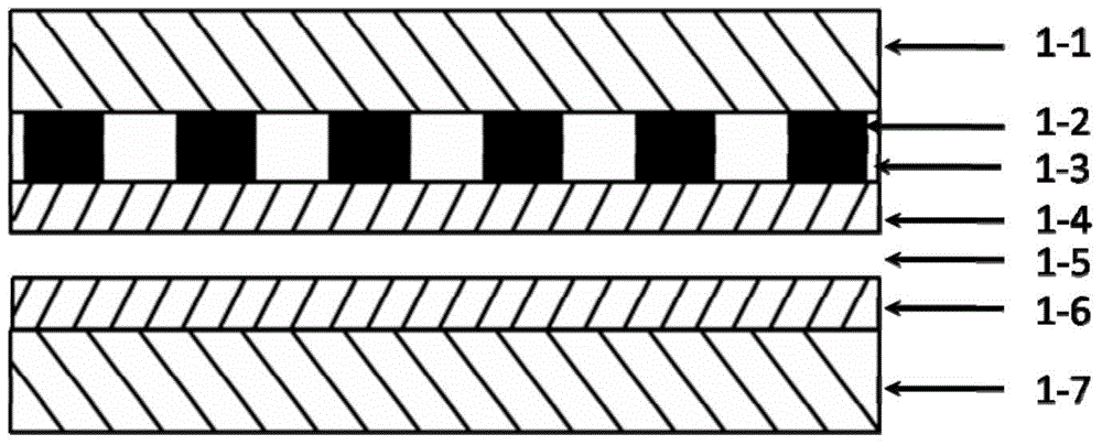
[0026] According to the principle of surface plasmon optics, the metal-medium-metal sandwich structure can be derived from Maxwell's equations to form a waveguide structure for transmitting light waves. The characteristics of the waveguide include: (1) light wave energy is transmitted along the metal-medium interface; (2) The waveguide mode is a resonant waveguide, that is, when other material parameters and geometric parameters are constant, the resonant conduction wavelength corresponds to the medium thickness parameter; (3) The waveguide transmission wave vector β is greater than the corresponding optical frequency in free space The wave vector β transmitted in 0 =2π / λ. The nano-gap detection structure, gap, and base structure in the present invention are as figure 1 As shown, 1-4 metal silver film layers, 1-6 metal silver film la...


PUM


Abstract

The invention provides a high precision nanometer clearance detection structure and method on the basis of surface plasma resonance, and belongs to the technical field of nanooptics. The high precision nanometer clearance detection structure and method on the basis of the surface plasma resonance can solve the problems that measuring precision is low and dynamic measurement cannot be carried out in the prior art. Light output by a light source enters a beam splitter through a collimating mirror and a broadband polarizer; the transmission light passing through the beam splitter interacts with the nanometer clearance detection structure and a substrate and then is reflected to the beam splitter; the light enters a spectrum detector after being reflected by the beam splitter and converged by a lens, the detector transmits obtained data through detection to a computer, clearance values are obtained through the processing of the computer, and the detection of the nanometer clearance is achieved. According to the high precision nanometer clearance detection structure and method on the basis of the surface plasma resonance, the method of spectrum detection is adopted to achieve high precision dynamic detection of a nanometer level clearance, a brand new testing technology is provided for the field of nanometer machining and nanometer measuring, and hopefully, the high precision nanometer clearance detection structure and method on the basis of the surface plasma resonance can play an important role in multiple fields including near-field optics and near-field physics.

Description

technical field [0001] The invention relates to the manufacture of a high-precision nano-gap detection structure based on surface plasmon resonance and the control of light waves, which can realize high-precision dynamic detection of nano-level gaps. Background technique [0002] The sensing and detection of nanoscale gap width is widely used in the fields of semiconductor manufacturing, high-density magnetic storage, and roughness detection of ultra-smooth surfaces. Especially in the field of near-field lithography, such as surface plasmon nano-lithography, scanning probe lithography, proximity X-ray lithography and other new nano-processing fields, in order to achieve high resolution and high processing accuracy, the device and substrate The pitch is usually required to be on the order of sub-micron or even tens of nanometers, and the gap accuracy needs to be controlled in the range of several nanometers to tens of nanometers. In order for the system to achieve such a high...

Claims


Application Information

Patent Timeline
Patent Type & Authority Patents(China)
IPC IPC(8): G01B11/14
Inventor 罗先刚王长涛王彦钦赵泽宇胡承刚蒲明薄李雄黄成何家玉罗云飞
Owner INST OF OPTICS & ELECTRONICS - CHINESE ACAD OF SCI
Why Eureka
Try Eureka