Optimization processing method for preparation of SERS substrate based on FIB direct-writing processing

A processing method and substrate technology, applied in digital control, gaseous chemical plating, electrical program control, etc., can solve problems affecting processing accuracy, difficult to process structural characteristics and stability maintenance, and difficult to obtain microstructure, etc., to achieve guaranteed Stability, guarantee of high flexibility, effect of improving sensitivity

Inactive Publication Date: 2015-04-29
TIANJIN UNIV
View PDF1 Cites 0 Cited by
  • Summary
  • Abstract
  • Description
  • Claims
  • Application Information

AI Technical Summary

Problems solved by technology

However, the texture of the thin noble metal layer evaporated on the substrate is softer than the substrate itself, and because the ion beam has a certain beam spot size, it will have a broadening effect during processing, which affects its processing accuracy, so the ion beam is directly deposited on the surface of the noble metal. Etching is difficult to maintain the characteristics and stability of the processed structure, and it is difficult to obtain a fine structure with a gap of less than 20nm

Method used


Image

  • Optimization processing method for preparation of SERS substrate based on FIB direct-writing processing
  • Optimization processing method for preparation of SERS substrate based on FIB direct-writing processing
  • Optimization processing method for preparation of SERS substrate based on FIB direct-writing processing

Examples


Embodiment Construction

[0024] The present invention will be further described below in conjunction with the accompanying drawings and embodiments.

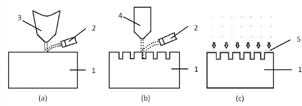
[0025] see figure 1 Firstly, the monocrystalline silicon sample substrate 1 is placed in the sample chamber of the dual-beam system, and the morphology of the sample is observed by the electron beam imaging system 3 . Using the focused ion beam 2 to perform ion etching processing on the single crystal silicon sample substrate 1 according to the target pattern, the focused ion beam etching parameters are adjusted according to the pattern and size, and on the basis of considering the broadening effect of the ion beam and combining the coating process parameters, A certain processing width is reserved, the accelerating voltage is controlled between 10kV-50kV, and the ion beam operating current is between 1pA-20nA, and then the electron beam imaging system 3 is used to observe whether the processed surface 4 meets the requirements of the experimental design...


PUM


Abstract

The invention relates to an optimization processing method for preparation of an SERS substrate based on FIB direct-writing processing. A focused ion beam (FIB)- electron beam two-beam system capable of carrying out electron beam scanning (SEM) and focused ion beam (FIB) processing is utilized. The method comprises the following steps: arranging a substrate to be processed in a two-beam system sample room and carrying out shape observation through an electron beam imaging system; preserving a certain processing width, and carrying out ion etching processing on the substrate by utilizing the focused ion beam (FIB) according to a target graph; utilizing the electron beams or the electron beam scanning imaging system to observe the processing process and result in real time; taking the sample out of the sample room and putting coating equipment in; and adjusting parameters with the ion beam processing structure and size being combined and vapor plating a precious metal film on the surface of the processing sample precisely, and taking the sample plated with the film as the surface enhanced Raman scattering (SERS) base. According to the method in the invention, the sensitivity and stability of the SERS base can be substantially improved.

Description

technical field [0001] The invention relates to a micro-nano processing method, more specifically, a micro-nano processing method for preparing SERS substrates based on focused ion beam and coating technology, which can be used for single-molecule detection, biological science sensing, and chemical analysis detection , micro-nano manufacturing, archaeological analysis, spectroscopy and other fields. Background technique [0002] With the discovery and principle research of localized surface plasmon resonance, the SERS active substrate based on LSPR technology has been rapidly developed and developed. The physical parameters of the micro-nano structure on the surface of the substrate, such as material, size, and shape, have become the core issues of processing and research. , and more and more methods have been used to prepare active SERS substrates. However, obtaining a SERS substrate with both high sensitivity and high stability is still a barrier to the widespread applica...

Claims


Application Information

Patent Timeline
Patent Type & Authority Patents(China)
IPC IPC(8): G05B19/18B81C1/00
Inventor 徐宗伟李康房丰洲高婷婷申雪岑徐晓轩
Owner TIANJIN UNIV
Why Eureka
Try Eureka