Silicon photomultiplier detector
A detector and silicon photoelectric technology, which is applied in the direction of circuits, electrical components, semiconductor devices, etc., can solve the problems of pixel size limitation, lack of position sensitivity limitation, and low gain of sensitive detectors.
- Summary
- Abstract
- Description
- Claims
- Application Information
AI Technical Summary
Problems solved by technology
Method used
Image

Examples
Embodiment Construction
[0014] The present invention takes the following technical solutions:
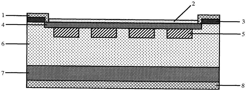
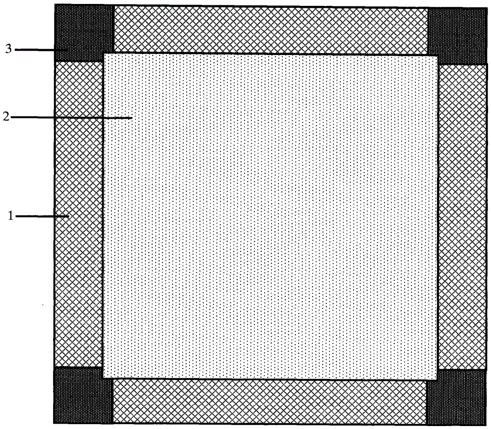
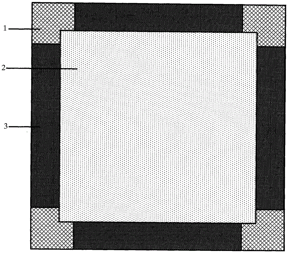
[0015] 1. A silicon photomultiplier detector, composed of 100,000 to 100,000 avalanche photodiode (APD) units integrated on the same silicon epitaxial wafer, the front electrode is located on the surface of the device, and the back electrode is on the side of the silicon substrate. direction, the APD units are isolated by the deep depletion region of the surrounding PN junction, and in the longitudinal direction, each APD unit is connected in series with an avalanche quenching resistor, and the avalanche quenching resistor is prepared from the epitaxial layer of the silicon epitaxial wafer , all APD units are connected by a uniform and continuous heavily doped silicon resistance layer on the device surface, and the heavily doped silicon resistance layer is used as a shunt resistance of a position-sensitive detector, which is characterized by:
[0016] The front electrode is composed of four independent ele...
PUM
 Abstract
Description
Claims
Application Information
 - R&D Engineer
- R&D Manager
- IP Professional
- Industry Leading Data Capabilities
- Powerful AI technology
- Patent DNA Extraction
Browse by: Latest US Patents, China's latest patents, Technical Efficacy Thesaurus, Application Domain, Technology Topic.
© 2024 PatSnap. All rights reserved.Legal|Privacy policy|Modern Slavery Act Transparency Statement|Sitemap