
Preparation method for realizing graphical ZnO nanowire arrays by micro-contact printing

A nanowire array and patterning technology, which is applied in the direction of nanostructure manufacturing, pattern surface photolithography, nanotechnology, etc., can solve the problems of poor quality of ZnO nanowires, large pattern size, harsh conditions, etc., and achieve clear patterns , the effect of small cell size

Inactive Publication Date: 2014-09-10
XI AN JIAOTONG UNIV
View PDF6 Cites 6 Cited by
  • Summary
  • Abstract
  • Description
  • Claims
  • Application Information

AI Technical Summary

Problems solved by technology

[0006] The purpose of the present invention is to prepare patterned ZnO nanowire arrays by physical methods such as photolithography and ion beam focused etching, which require advanced equipment, time-consuming, harsh conditions, and precious metal catalysis, and to prepare OTS monomolecular layers by microcontact imprinting. In order to solve the problems of poor quality and large pattern size of ZnO nanowires grown on patterned seed layer of ZnO nanocrystals, a method for preparing patterned ZnO nanowire arrays by microcontact imprinting is provided.

Method used


Image

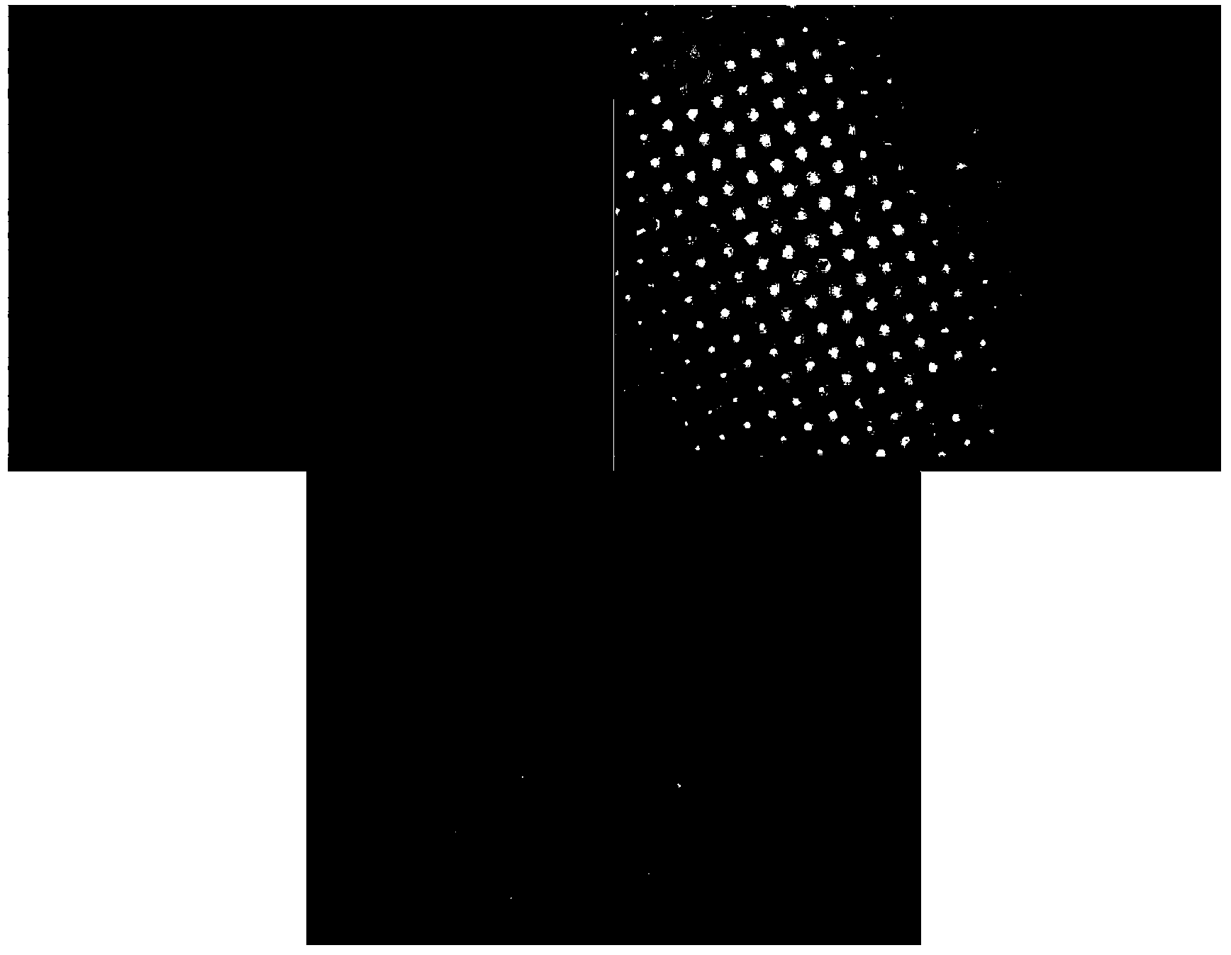
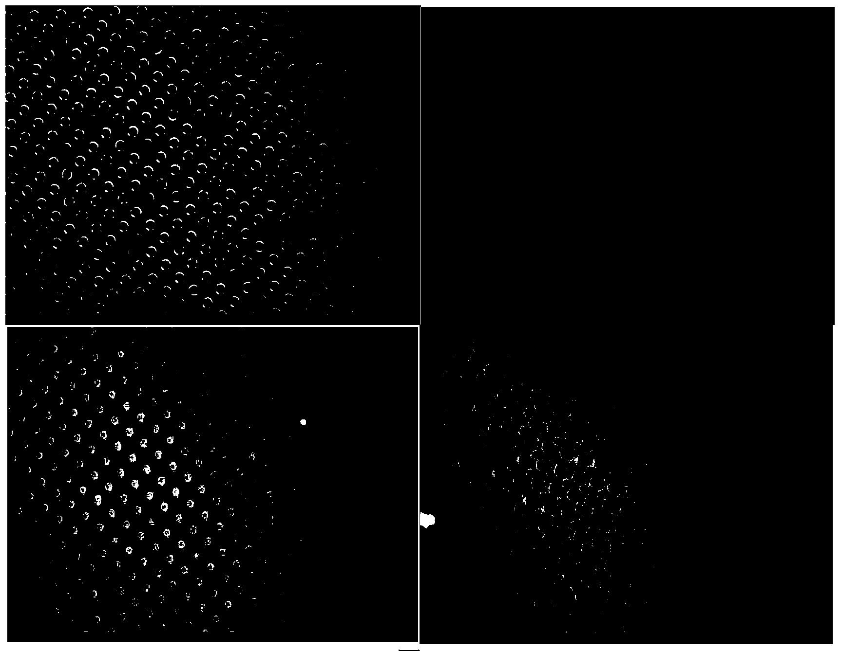
  • Preparation method for realizing graphical ZnO nanowire arrays by micro-contact printing
  • Preparation method for realizing graphical ZnO nanowire arrays by micro-contact printing
  • Preparation method for realizing graphical ZnO nanowire arrays by micro-contact printing

Examples


Embodiment Construction

[0020] The present invention will be further described below in conjunction with examples, but not intended to limit the present invention.

[0021] Example:

[0022] The preparation of ZnO seed layer thin film: first prepare the ethanol solution of 5mmol / L zinc acetate, take ITO conductive glass as the substrate, adopt 2000rmp, 30s spin process continuous spin coating 5 times; heat treatment repeated 2 times); finally put it into a furnace to raise the temperature to 300°C at a rate of 3°C / min, and anneal at this temperature for 0.5-1h to obtain a ZnO seed layer.

[0023] TiO 2 Preparation of sol ink: first, add 4ml of tetrabutyl titanate dropwise to 16ml of ethylene glycol methyl ether under magnetic stirring, and stir evenly; then add 2.5ml of diethanolamine dropwise, and stir magnetically for a long time until mixed uniform.

[0024] The preparation of the patterned ZnO seed layer: first the size is 0.25cm 2 The elastic PDMS stamp was ultrasonically cleaned in absolute...


PUM


Abstract

The invention discloses a preparation method for micro-sized and graphical ZnO nanowire arrays by adopting two steps of micro-contact printing (MCP) and low-temperature chemical bath deposition (CBD). The preparation method includes: firstly, adopting a sol-gel method to prepare a ZnO seed layer film on conductive glass; transferring TiO2 sol ink to the ZnO seed layer film through elastic polydimethylsiloxane (PDMS) stamps with different graphics to acquire a graphical TiO2 shielding layer film; adopting a chemical bath deposition method to complete select growth of ZnO nanowires in a ZnO seed layer area shielded by the TiO2 film. The preparation method is simple in process, low in cost, large in preparation area and good in repeatability; the three critical techniques in the entire process refer to preparation of the TiO2 sol ink with appropriate viscosity, setting of inkiness of the PDMS stamps and pressure parameter of the printing process and time control of hydrothermal growth of the nanowires.

Description

technical field [0001] The invention belongs to the technical field of micro-nano manufacturing, and in particular relates to a method for preparing patterned ZnO nanowire arrays realized by micro-contact embossing. Background technique [0002] In recent years, one-dimensional ZnO nanowires, as an important functional oxide semiconductor material, have attracted people due to their application potential in optoelectronic devices, near-ultraviolet light-emitting devices, flat panel displays based on field emission, and self-assembled three-dimensional nanoscale systems. More and more attention. Studies on the orientation, size, and deposition location of ZnO nanowires have been widely reported. In order to realize structured electronic devices, the development of microstructure patterned ZnO nanowire arrays has become inevitable, and the realization of microstructure will be of great significance to the performance improvement and characteristic development of the above dev...

Claims


Application Information

Patent Timeline
IPC IPC(8): B82B3/00G03F7/00B82Y40/00
Inventor 汪敏强邓建平
Owner XI AN JIAOTONG UNIV
Learn More