Patterning method for graphene film

A graphene film and patterning technology, which is applied in the direction of electrical components, semiconductor/solid-state device manufacturing, circuits, etc., can solve the problems of excessive environmental equipment requirements, inability to use large-scale production, and poor effect of patterning methods, etc., to achieve production Low cost, elimination of adverse effects, and high processing efficiency

Inactive Publication Date: 2014-09-17
CHONGQING GRAPHENE TECH +1
View PDF7 Cites 9 Cited by
  • Summary
  • Abstract
  • Description
  • Claims
  • Application Information

AI Technical Summary

Problems solved by technology

[0003] Patterning is an essential link in the manufacture of semiconductor devices using graphene. Due to the extremely stable chemical properties of graphene, the effect of ordinary acid-base etching patterning is poor, and the plasma etching method has too high requirements for environmental equipme

Method used


Image

  • Patterning method for graphene film
  • Patterning method for graphene film
  • Patterning method for graphene film

Examples


Embodiment 1

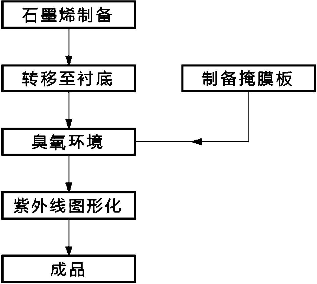
[0028] The patterning method of the graphene thin film of the present embodiment comprises the following steps:

[0029] 1), preparing a graphene film and transferring it to a substrate;

[0030] Firstly, a chemical vapor deposition method is used to grow a graphene film on a metal film, and the metal film is copper foil, aluminum foil or nickel foil; then the obtained graphene film is transferred to a PET film substrate.

[0031] 2), making a graphene mask;

[0032] A mask is prepared according to the desired pattern, and the mask in this embodiment is a hollowed-out tinfoil mask.

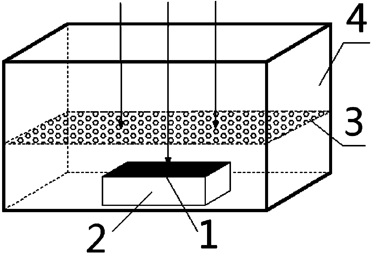
[0033] 3), the graphene mask plate and the graphene film are placed in an ozone environment;

[0034] When placing, pay attention to placing the mask plate between the graphene film and the ultraviolet light source.

[0035] 4) Graphicalization: turn on the ultraviolet light source and graphene film; figure 2 It is a schematic diagram of the graphical processing steps of the present embodimen...


PUM

PropertyMeasurementUnit
Wavelengthaaaaaaaaaa
Strengthaaaaaaaaaa

Abstract

The invention discloses a patterning method for a graphene film. According to the method, ultraviolet rays in an ozone environment pattern the graphene film through a graphene mask plate, and in detail, the method includes the following steps that firstly, the graphene film is manufactured and transferred to a substrate; then the graphene mask plate is manufactured; then the graphene mask plate and the graphene film are placed in the ozone environment; finally, in the ozone environment, the graphene film is patterned through the graphene mask plate. The patterning method for the graphene film is not only low in production cost, but also high in machining efficiency, and significant technical barriers are cleared for industrialized application of graphene.

Description

technical field [0001] The invention belongs to the field of semiconductor devices and relates to a method for patterning a graphene film. Background technique [0002] Graphene has excellent comprehensive physical and chemical properties, and has attracted much attention since its inception; the sheet resistance of single-layer graphene is as low as 5Ω / sq, the light transmittance of the whole band is higher than 97%, and it has extremely high electron mobility. It still maintains good electrical characteristics in the limit size line; it has become an important substitute for silicon in the semiconductor field and has broad application prospects. [0003] Patterning is an essential link in the manufacture of semiconductor devices using graphene. Due to the extremely stable chemical properties of graphene, the effect of ordinary acid-base etching patterning is poor, and the plasma etching method has too high requirements for environmental equipment and cannot be used for La...

Claims


Application Information

Patent Timeline
IPC IPC(8): H01L21/02G03F7/42
CPCH01L21/042H01L21/26
Inventor 潘洪亮崔华亭史浩飞余崇圣张为国钟达
Owner CHONGQING GRAPHENE TECH
Why Eureka
Try Eureka