Manufacturing technology of bionic solar cell with two sides receiving light

A solar cell and manufacturing process technology, applied in the field of solar cells, can solve the problems of reducing reflectivity and emitter passivation, unfavorable conversion efficiency of crystalline silicon cells, unfavorable indoor environmental beautification of grid lines, etc., to increase long-wave response and increase field Passivation effect, effect that facilitates collection

Active Publication Date: 2014-09-17
REALFORCE POWER
View PDF3 Cites 9 Cited by
  • Summary
  • Abstract
  • Description
  • Claims
  • Application Information

AI Technical Summary

Problems solved by technology

[0002] At present, crystalline silicon solar cells generally use silicon nitride film for anti-reflection on the front side, and aluminum back field passivation on the back side. The silicon nitride film plays the role of reducing reflectivity and passivating the emitter. Poor, the passivation effect is not good; the aluminum back field is the P+ layer formed during the sintering process, which can reflect the minority carriers---electrons, and play a passivation role, but the field strength of the aluminum back field is relatively weak, and it is harmful to The reflection of long-wave photons is low, which is not conducive to further improving the conversion efficiency of crystalline silicon cells. On the other hand, the current double-sided crystalline silicon cells are printed with regular grid lines. When double-glass modules are applied to photovoltaic curtain walls, rigid grids Lines are not conducive to the beautification of the indoor environment

Method used


Image

  • Manufacturing technology of bionic solar cell with two sides receiving light
  • Manufacturing technology of bionic solar cell with two sides receiving light
  • Manufacturing technology of bionic solar cell with two sides receiving light

Examples


Embodiment Construction

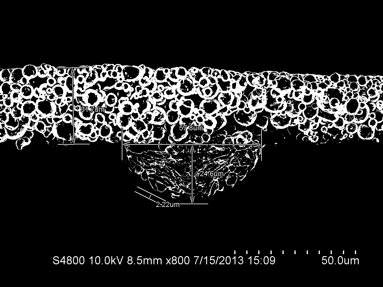
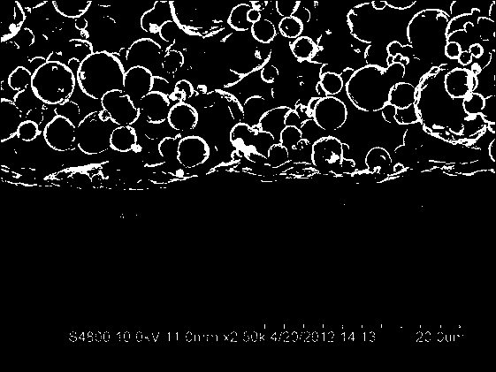
[0023] like Figure 1-3 As shown, a manufacturing process of a bionic double-sided light-receiving solar cell adopts the following sequential process steps:

[0024] Step 1, texture the surface of the crystalline silicon wafer to reduce the surface reflectivity;

[0025] Step 2, the silicon wafer after texturing is passed through the phosphorus source and pushed forward, this step only carries out the source flow process, and does not carry out the push process;

[0026] Step 3, performing wet etching on the diffused silicon wafer to remove the back N+ layer;

[0027] Step 4, performing atomic layer deposition on the silicon wafer after wet etching, so that a layer of aluminum oxide film is grown on the back of the silicon wafer;

[0028] Step 5, the atomic layer deposited silicon wafer is subjected to an oxygen-passing annealing process in a high-temperature tube to remove the residual methyl groups in the aluminum oxide film, and at the same time thermally oxidize the surf...


PUM

PropertyMeasurementUnit
thicknessaaaaaaaaaa
thicknessaaaaaaaaaa
thicknessaaaaaaaaaa

Abstract

The invention provides a manufacturing technology of a bionic solar cell with the two sides receiving light. The manufacturing technology comprises the nine steps of texture surface making, diffusion, etching on the back side, aluminum oxide deposition on an atomic layer, oxygen feeding and annealing, silicon nitride growing, laser film opening, printing and sintering. An aluminum oxide film depositing on the atomic layer is used on the back side of a passivated cell. Silicon nitride generated through thermal oxidation is used on the front side of the passivated cell. Reconstruction of the aluminum oxide film, formation of an oxide layer on the front side and further advancement of an emitter junction are completed through the annealing technology. A traditional aluminum back surface field technology is replaced by aluminum grid line printing on the back side, so that the field passivation effect of aluminum oxide is improved, and an open-circuit voltage is increased. In addition, reflection of long-wave photons on the back side is increased through back side laminated films, so that the long-wave response of the crystalline silicon cell is improved. Besides, the bionic tree leaf grid line structure on the back side facilitates collection of back side scattering photons, and an excellent cell structure is provide for a double-glass assembly; meanwhile, the indoor environment of a curtain wall is beautified.

Description

technical field [0001] The invention relates to a solar cell, in particular to a manufacturing process of a bionic double-sided light-receiving solar cell with greatly improved light conversion efficiency. Background technique [0002] At present, crystalline silicon solar cells generally use silicon nitride film for anti-reflection on the front side, and aluminum back field passivation on the back side. The silicon nitride film plays the role of reducing reflectivity and passivating the emitter. Poor, the passivation effect is not good; the aluminum back field is the P+ layer formed during the sintering process, which can reflect the minority carriers---electrons, and play a passivation role, but the field strength of the aluminum back field is relatively weak, and it is harmful to The reflection of long-wave photons is low, which is not conducive to further improving the conversion efficiency of crystalline silicon cells. On the other hand, the current double-sided crys...

Claims


Application Information

Patent Timeline
Patent Type & Authority Applications(China)
IPC IPC(8): H01L31/18
CPCH01L31/022433H01L31/1804H01L31/1868Y02E10/547Y02P70/50
Inventor 孟祥海钱金梁孙广印陈斌王步峰
Owner REALFORCE POWER
Why Eureka
Try Eureka