Manufacturing method of odd-numbered layer substrate and odd-numbered layer substrate
A manufacturing method and technology of odd-numbered layers, applied in the field of microelectronics, to achieve the effects of reducing thickness, realizing no-hole electroplating, and reducing aspect ratio
- Summary
- Abstract
- Description
- Claims
- Application Information
AI Technical Summary
Problems solved by technology
Method used
Image

Examples
Embodiment 1
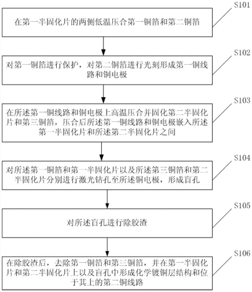
[0051] figure 1 It is a flow chart of a method for manufacturing an odd-numbered-layer substrate provided in Embodiment 1 of the present invention. The method includes steps S101 to S106. It should be noted that the steps in this embodiment are named after steps S101 to S106 for convenience only. The steps are distinguished, but the order of the steps is not limited. In different embodiments of the present invention, the order of the steps can be adjusted according to the adjustment of the process.
[0052] Step S101 , low-temperature pressure-bonding of the first copper foil and the second copper foil on both sides of the first prepreg.
[0053] Step S102 , protecting the first copper foil, and performing photolithography on the second copper foil to form first copper lines and copper electrodes.
[0054] In this embodiment, the first copper line and the copper electrode can be interconnected according to the needs of circuit design, and blind holes can be drilled on the cop...
Embodiment 2
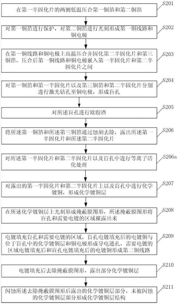
[0068] figure 2 It is a flow chart of a method for manufacturing an odd-numbered-layer substrate provided in Embodiment 2 of the present invention, Figures 3A-3J It is a schematic structural cross-sectional diagram corresponding to each step of an odd-numbered-layer substrate manufacturing method provided by Embodiment 2 of the present invention. This embodiment is based on the above-mentioned embodiment, and adopts a semi-additive method when manufacturing the second copper circuit. The method includes step S201 to step S211. It should be noted that, in this embodiment, the steps are named from step S201 to step S211 only for the convenience of distinguishing the steps, rather than limiting the order of the steps. In different implementations of the present invention In the example, the sequence of each step can be adjusted according to the adjustment of the process. The following will combine Figure 3A to Figure 3J Each step from S201 to S211 will be described according...
Embodiment 3
[0102] Figure 4 It is a flowchart of a method for manufacturing an odd-numbered-layer substrate provided in Embodiment 3 of the present invention, Figures 5A-5B It is a schematic structural cross-sectional diagram corresponding to each step of an odd-numbered-layer substrate manufacturing method provided by Embodiment 3 of the present invention. This embodiment is based on Embodiment 2. The difference from Embodiment 2 is that the three-layer Substrate. In this embodiment, a multi-layer odd-numbered-layer substrate can be manufactured. Specifically, the method for manufacturing the odd-numbered-layer substrate further includes:
[0103] Step S312 , high-temperature pressing and curing the third prepreg and the fourth copper foil respectively on the electroplated copper lines on both sides of the substrate, wherein the thickness of the fourth copper foil is 2 μm.
[0104] see Figure 5A 1. On the basis of the three-layer substrate manufactured in the first embodiment, the t...
PUM
| Property | Measurement | Unit |
|---|---|---|
| thickness | aaaaa | aaaaa |
| thickness | aaaaa | aaaaa |
| thickness | aaaaa | aaaaa |
Abstract
Description
Claims
Application Information
 - R&D
- Intellectual Property
- Life Sciences
- Materials
- Tech Scout
- Unparalleled Data Quality
- Higher Quality Content
- 60% Fewer Hallucinations
Browse by: Latest US Patents, China's latest patents, Technical Efficacy Thesaurus, Application Domain, Technology Topic, Popular Technical Reports.
© 2025 PatSnap. All rights reserved.Legal|Privacy policy|Modern Slavery Act Transparency Statement|Sitemap|About US| Contact US: help@patsnap.com