Planar optical element and design method thereof
An optical element and plane technology, applied in the field of optics, can solve the problems of weak spin Hall effect, complex observation system, unfavorable intuitive observation, etc., to achieve reliable design methods and the effect of filling vacancies
- Summary
- Abstract
- Description
- Claims
- Application Information
AI Technical Summary
Problems solved by technology
Method used
Image
Examples
Embodiment Construction
[0032] The technical solutions of the present invention will be described in further detail below with reference to the accompanying drawings and embodiments.
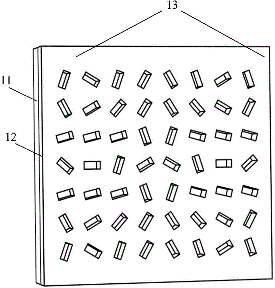
[0033] The embodiments of the present invention design a planar optical element with an antenna microarray with a specific structure, and realize polarization separation of circularly polarized light.
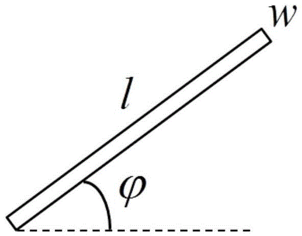
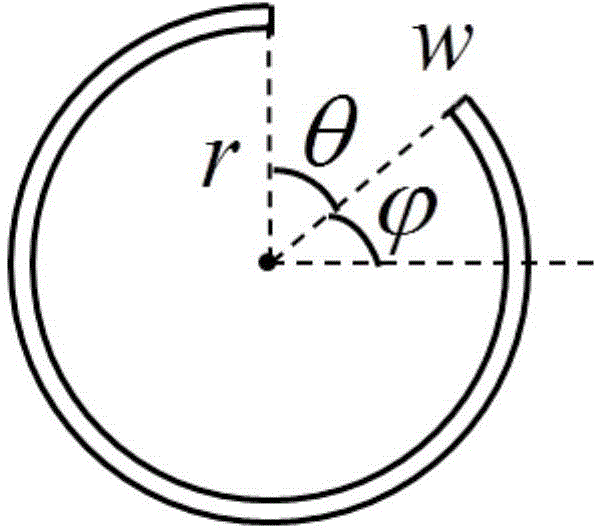
[0034] figure 1 It is a partial structural schematic diagram of the planar optical element of the embodiment of the present invention. The planar optical element can be used to realize the polarization separation of the circularly polarized light in the whole wavelength range. As shown in the figure, the planar optical element includes: a substrate 11 and a metal film 12 . The material of the substrate 11 is a material with high transmittance for the used light band, such as silicon semiconductor, gallium arsenide semiconductor, and the thickness ranges from 300 μm to 1000 μm. The metal film 12 can be a good conducto...
PUM
 Abstract
Description
Claims
Application Information


