Composition Of An Aqueous Etchant Containing A Precursor Of Oxidant And Patterning Method For Conductive Circuit
A conductive circuit and etchant technology, which is applied in the field of aqueous etchant composition, conductive circuit structure and conductive circuit patterned preparation, to achieve the effects of simplifying the preparation method, reducing the production cost and being easy to control.
- Summary
- Abstract
- Description
- Claims
- Application Information
AI Technical Summary
Problems solved by technology
Method used
Image
Examples
Embodiment 1
[0027] Embodiment 1: applied to electronic devices
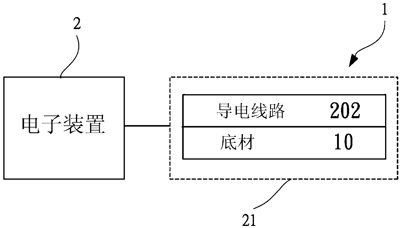
[0028] Such as figure 1 As shown, the conductive substrate 1 can be applied to an electronic device 2 with a sensor 21 (Sensor) function to electrically connect the conductive substrate 1 formed by an aqueous etchant of a strong oxide precursor; in addition, the conductive The base material 1 can also be applied to include printed electronics (Printed Electronics), sensor (Sensor), display (Display), organic light emitting diode (OLED), touch panel (Touch Panel), electronic circuit board (Electronic Circuit Board), electrode (Electrode), EL (EL), Antenna (Antenna), Solar Cell (Solar Cell) and other electronic devices with different functions.
Embodiment 2
[0029] Embodiment 2: Utilize aqueous etchant of the present invention to carry out the preparation method of patterning conductive layer
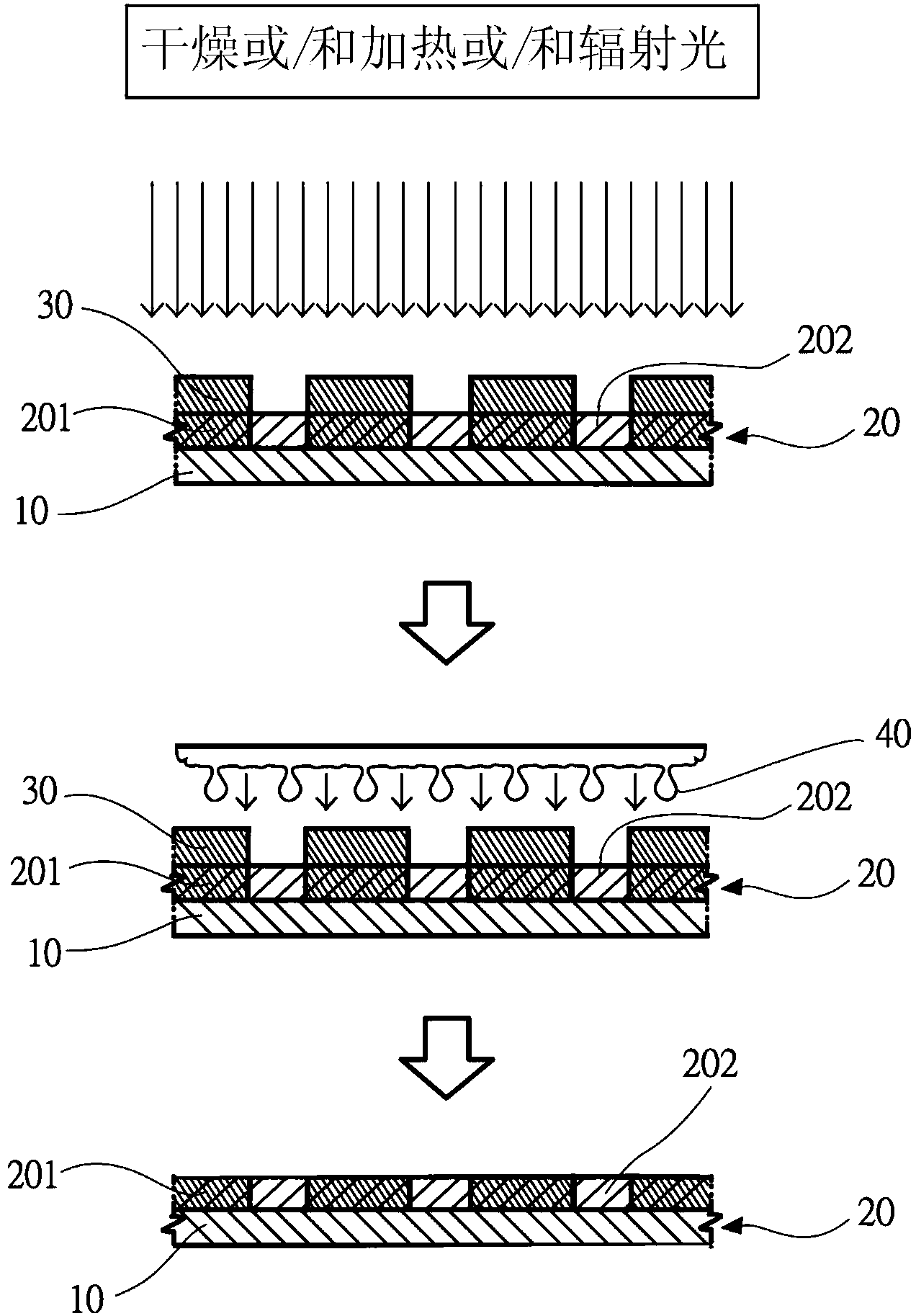
[0030] Such as figure 2 As shown in the figure of the embodiment of the preparation method of the present invention, the specific preparation method for patterning the conductive layer using the aqueous etchant of the chlorine-containing strong oxide precursor of the strong oxide includes:
[0031] Covering the surface of the substrate 10 with a conductive layer 20 composed of a conjugated intrinsically conductive conductive polymer;
[0032] Covering a layer of etchant layer 30 made of the aqueous etchant on a specific (Predetermined) area on the surface of the conductive layer 20 that needs to be oxidized;
[0033] Use any one or combination of drying, heating or radiating light to make the strong oxide precursor produce a strong oxide, and perform etching by oxidizing the contacted conductive layer 20, so that the electrical resistance...
Embodiment 3
[0035] Embodiment 3: Etching the conductive layer by irradiation with radiant light
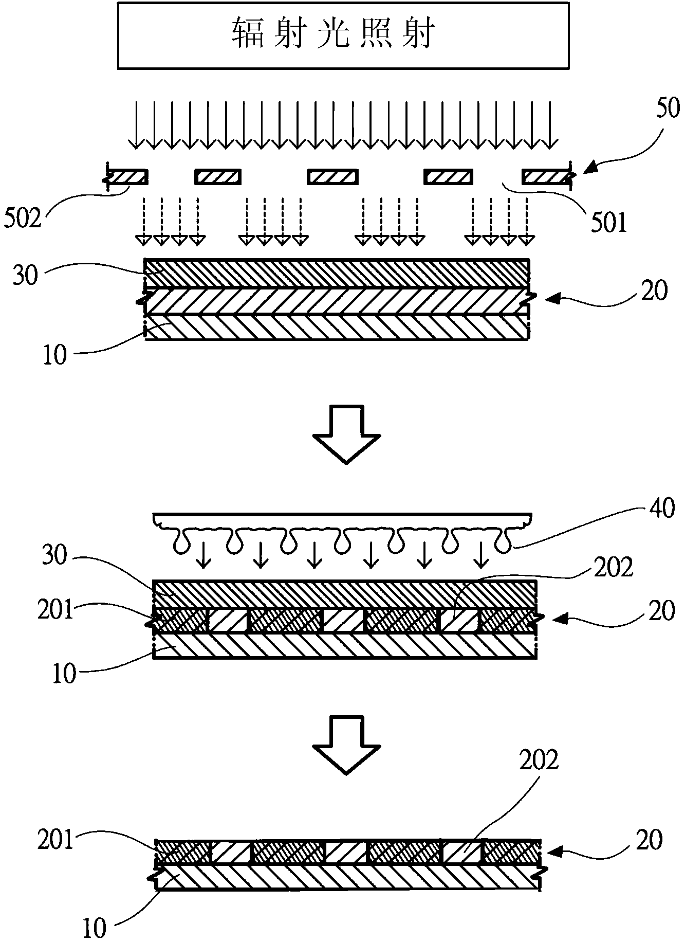
[0036] Such as image 3 As shown, the strong oxide produced by the irradiation of radiant light to oxidize the contacted conductive layer 20 for etching can be further irradiated through a photomask (Photo Mask) 50, and the photomask 50 defaults to The light-transmitting region 501 that needs to be oxidized for patterning, and the non-transmitting region 502 that does not need to be oxidized, achieve radiation light irradiating the etchant layer 30 through the light-transmitting region 501 of the mask 50, so that the etchant that is irradiated by the radiated light The strong oxide precursor of layer 30 produces a strong oxide that etches by oxidizing the contacted conductive layer 20 to form non-conductive regions 201, while the regions not exposed to radiant light and shaded by non-transmissive regions 502 form conductive lines 202. The wavelength of the aforementioned radiated light is a...
PUM
| Property | Measurement | Unit |
|---|---|---|
| wavelength | aaaaa | aaaaa |
Abstract
Description
Claims
Application Information


