Ohmic contact production method of aluminum gallium nitride and gallium nitride HEMT (High Electron Mobility Transistor)

A high electron mobility, ohmic contact technology, applied in semiconductor/solid-state device manufacturing, circuits, electrical components, etc., can solve the problems of difficult ohmic contact, increased contact resistance, etc., and achieve smooth metal topography, better edge, edge neat effect

Active Publication Date: 2014-10-22
NO 55 INST CHINA ELECTRONIC SCI & TECHNOLOGYGROUP CO LTD
View PDF4 Cites 9 Cited by
  • Summary
  • Abstract
  • Description
  • Claims
  • Application Information

AI Technical Summary

Problems solved by technology

It should be said that increasing the Al content in AlGaN can increase the carrier concentration of the channel layer in AlGaN / GaN HEMTs, which in turn helps to improve the performance of the device; but the higher the Al content in the AlGaN layer, the more difficult it is to form with the metal. Ohmic contact, when the Al content exceeds 0.3, the contact resistance increases significantly

Method used


Image

  • Ohmic contact production method of aluminum gallium nitride and gallium nitride HEMT (High Electron Mobility Transistor)
  • Ohmic contact production method of aluminum gallium nitride and gallium nitride HEMT (High Electron Mobility Transistor)
  • Ohmic contact production method of aluminum gallium nitride and gallium nitride HEMT (High Electron Mobility Transistor)

Examples


Embodiment 1

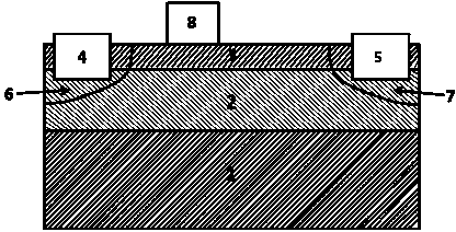
[0063] Non-alloy ohmic contact embodiment 1, source and drain etching of photoresist mask

[0064] Coating photoresist 17 on sheet surface, as Figure 12 shown. The pattern is defined by exposure and development. The etched area is within the implanted area and smaller than the implanted area. The distance between the boundary of the etched area and the implanted area is between 100 and 500 nm, forming a pattern such as Figure 13 structure shown. AlGaN and GaN are difficult to be wet etched, but they can be etched by Cl 2 etch away. Commonly used dry etching methods include RIE and ICP. Here, the ICP etching method is used to etch away the AlGaN barrier layer. After cleaning and degumming, it is formed as Figure 14 The structure shown, 18, represents the recessed region formed after the barrier layer has been etched away.

[0065] like Figure 15 As shown, the photoresist 19 is coated, exposed and developed to define source and drain patterns, such as Figure 16 show...

Embodiment 2

[0069] Non-alloy ohmic contact implementation 2, dielectric mask source and drain etching

[0070] The gas used in dry etching GaN and AlGaN is generally Cl-based gas, such as Cl 2 、BCl 3 etc.; while etching SiN usually uses F-based gases, such as SF 6 、CF 4 、CHF 3wait. Just based on the difference in etching selectivity between Cl-based and F-based gases for SiN and GaN (AlGaN), the present invention proposes to use SiN medium as the source-drain etching mask.

[0071] exist Figure 11 After removing the annealing protection medium, grow the SiN mask medium 28, such as Figure 21 shown. Coating photoresist 29 on sheet surface, as Figure 22 shown. The pattern is defined by exposure and development. The etched area is within the implanted area and smaller than the implanted area. The distance between the boundary of the etched area and the implanted area is between 100 and 500 nm, forming a pattern such as Figure 23 structure shown.

[0072] First, use F-based gase...


PUM

PropertyMeasurementUnit
thicknessaaaaaaaaaa
thicknessaaaaaaaaaa
thicknessaaaaaaaaaa

Abstract

The invention provides an ohmic contact production method of an aluminum gallium nitride and gallium nitride HEMT (High Electron Mobility Transistor). The ohmic contact production method comprises step 1, injecting doped ions in a designated area, activating the ions at the high temperature through annealing, defining graphics of the injection area by a lithography method, depositing a metal mask and performing stripping, enabling injection required positions to be exposed out, serving metal as a mask defined injection area during injection and serving silicon ions as injection ions and step 2, etching an aluminum gallium nitride barrier layer of part of the injection area and depositing the metal at the positions where the aluminum gallium nitride is etched to be in direct contact with a gallium nitride layer. According to the ohmic contact production method of the aluminum gallium nitride and gallium nitride HEMT, the ohmic contact resistivity can be low; a metal electrode is good in surface smoothness and reliability; the ohmic contact of the aluminum gallium nitride and gallium nitride HEMT can be achieved without an aluminum contained multilayer metal system and accordingly the damage of the follow-up process to the ohmic contact due to the fact that chemical properties of the aluminum metal are lively is avoided and the reliability of the ohmic contact is improved.

Description

technical field [0001] The invention relates to an ohmic contact manufacturing method of an AlGaN / GaN high electron mobility transistor, and is a new source-drain ohmic contact manufacturing method. It belongs to the field of semiconductor technology. Background technique [0002] High electron mobility transistors based on AlGaN / GaN heteroepitaxy structures have broad application prospects in high-frequency, high-power microwave communications, radar detection and other fields. The contact resistance between source and drain metal electrodes and semiconductor materials in aluminum gallium nitride (AlGaN) / gallium nitride (GaN) high electron mobility transistors (HEMT) directly affects the performance of output power, power added efficiency and frequency characteristics. How to reduce the contact resistance Resistance is an important factor that must be considered when fabricating high-performance AlGaN / GaN HEMT devices. Most of the ohmic contacts adopt a multilayer metal s...

Claims


Application Information

Patent Timeline
Patent Type & Authority Applications(China)
IPC IPC(8): H01L21/28
CPCH01L21/28575
Inventor 孙高峰任春江陈堂胜
Owner NO 55 INST CHINA ELECTRONIC SCI & TECHNOLOGYGROUP CO LTD
Why Eureka
Try Eureka