Optical coupling apparatus for packaging optoelectronic integration array chip

An array chip and optoelectronic technology, which is applied in the fields of microwave photonics and optical communication, can solve the problems that it is no longer applicable, the high frequency performance of the chip is also greatly affected, and there is not enough space for the placement of the backlight detector, so as to achieve real-time monitoring. Effect

Inactive Publication Date: 2014-10-29
INST OF SEMICONDUCTORS - CHINESE ACAD OF SCI
View PDF3 Cites 7 Cited by
  • Summary
  • Abstract
  • Description
  • Claims
  • Application Information

AI Technical Summary

Problems solved by technology

For some specific cases, in order to meet the high-frequency performance required by communication, a complex microwave microstrip circuit is placed on the back of the monolithic integrated multi-wavelength laser array chip, and there is not enough space to place a backlight detector.
If the microwave microstrip circuit is re-arranged, not only is the process complicated, but it also has a great impact on the high-frequency performance of the packaged monolithic integrated multi-wavelength laser array chip
In addition, for semiconductor optoelectronic device array chips that require double-ended coupling, such as optical modulator array chips, semiconductor optical amplifier array chips, etc., the scheme of arranging backlight detectors is no longer applicable.

Method used


Image

  • Optical coupling apparatus for packaging optoelectronic integration array chip
  • Optical coupling apparatus for packaging optoelectronic integration array chip

Examples


Embodiment Construction

[0013] In order to make the object, technical solution and advantages of the present invention clearer, the present invention will be described in further detail below in conjunction with specific embodiments and with reference to the accompanying drawings.

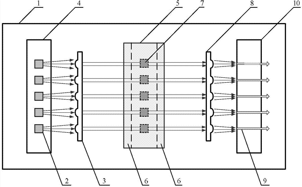
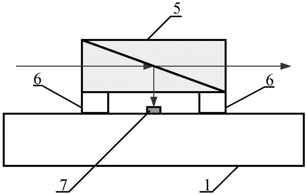
[0014] The invention proposes an optical coupling device applied to semiconductor optoelectronic integrated array chip packaging, figure 1 For a schematic diagram of the device, figure 2 It is a schematic diagram of the placement position of the detector array chip. exist figure 1 and figure 2 , the meanings of the reference signs are as follows:

[0015] 1-tube shell or heat sink; 2-semiconductor optoelectronic integrated array chip;

[0016] 3-Optical collimation lens array; 4-Semiconductor optoelectronic integrated array chip substrate;

[0017] 5-beam splitting prism; 6-beam splitting prism holder;

[0018] 7-detector array chip; 8-optical focusing lens array;

[0019] 9-fiber array; 10-fiber array bracket. ...


PUM


Abstract

The invention discloses an optical coupling apparatus for packaging an optoelectronic integration array chip. The optical coupling apparatus comprises a tube shell or a heat sink, the semiconductor optoelectronic integration array chip, a semiconductor optoelectronic integration array chip substrate, an optical collimating lens array, a beam splitter prism, a beam splitter prism bracket, detector array chips, an optical focusing lens array, a fiber array, and a fiber array bracket. According to the optical coupling apparatus for packaging the optoelectronic integration array chip, by means of installation of the beam splitter prism, partial optical signals output by the semiconductor optoelectronic integration array chip collimated by the optical collimating lens array are introduced into the respective corresponding detector array chips, so that difficulties that a backlight detector cannot be placed due to complicated microwave micro-strip circuits or the requirement for double-end optical coupling in coupling packaging of the semiconductor optoelectronic integration array chip are overcome, and real-time monitoring of optical signals of the semiconductor optoelectronic integration array chip is achieved.

Description

technical field [0001] The invention belongs to the technical field of microwave photonics and optical communication, and more specifically relates to an optical coupling device applied to semiconductor optoelectronic integrated array chip packaging. Background technique [0002] Optoelectronics integration technology is the most cutting-edge and promising field of optical fiber communication, and it is the main technology in the future high-speed and large-capacity information network system. Compared with traditional discrete devices, photonic integrated chips reduce cost and complexity, so a new network structure with more nodes can be built at a lower cost. [0003] The monolithic integrated multi-wavelength laser array chip is the core of realizing high-speed data transmission, and the coupling packaging of the monolithic integrated multi-wavelength laser array chip is particularly important. Usually, it is necessary to install a detector on the back of the semiconduct...

Claims


Application Information

Patent Timeline
Patent Type & Authority Applications(China)
IPC IPC(8): G02B6/43G02B6/34G02B6/32
Inventor 王欣邓晔刘建国祝宁华
Owner INST OF SEMICONDUCTORS - CHINESE ACAD OF SCI
Why Eureka
Try Eureka