Method for forming semiconductor structure

A semiconductor and bulk substrate technology, applied in the fields of semiconductor devices, semiconductor/solid-state device manufacturing, electrical components, etc., can solve the problem of inconsistent electrical properties of several fin field effect transistors, difficult to control the thickness and size of the gate structure, and difficult performance of semiconductor devices. Control and other issues to achieve the effect of improving stability, uniform thickness, and uniform thickness and size

Active Publication Date: 2014-10-29
SEMICON MFG INT (SHANGHAI) CORP
View PDF4 Cites 12 Cited by
  • Summary
  • Abstract
  • Description
  • Claims
  • Application Information

AI Technical Summary

Problems solved by technology

[0005] However, in the prior art, when a fin field effect transistor with a high-K metal gate structure is formed by a post-gate process, the thickness of the gate structure on the top surface of several fins on the same semiconductor substrate is not uniform, and the g...

Method used


Image

  • Method for forming semiconductor structure
  • Method for forming semiconductor structure
  • Method for forming semiconductor structure

Examples


Embodiment Construction

[0035] As mentioned in the background, the thickness of the gate structure on the top surface of the fin in the prior art is non-uniform and imprecise.

[0036] In one embodiment, the formation process of forming the high-K metal gate structure on the surface of the fin is as follows: Figure 2 to Figure 4 shown.

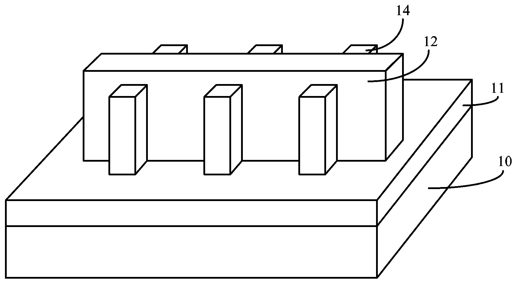
[0037] Please refer to figure 2 , providing a semiconductor substrate 10, a protruding fin 14 located on the semiconductor substrate 10, and a dielectric layer 11 covering the surface of the semiconductor substrate 10 and part of the sidewall of the fin 14, on the surface of the dielectric layer 11 and the fin The dummy gate layer 15 is deposited on the sidewalls and top surfaces of fins 14 , and the dummy gate layer 15 fills the openings (not shown) between adjacent fins 14 .

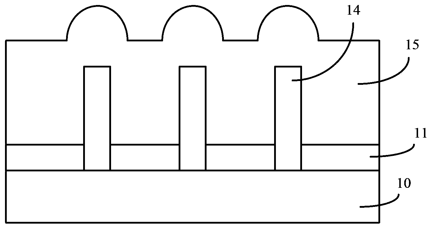
[0038] Please refer to image 3 , using a chemical mechanical polishing process to planarize the dummy gate layer 15 .

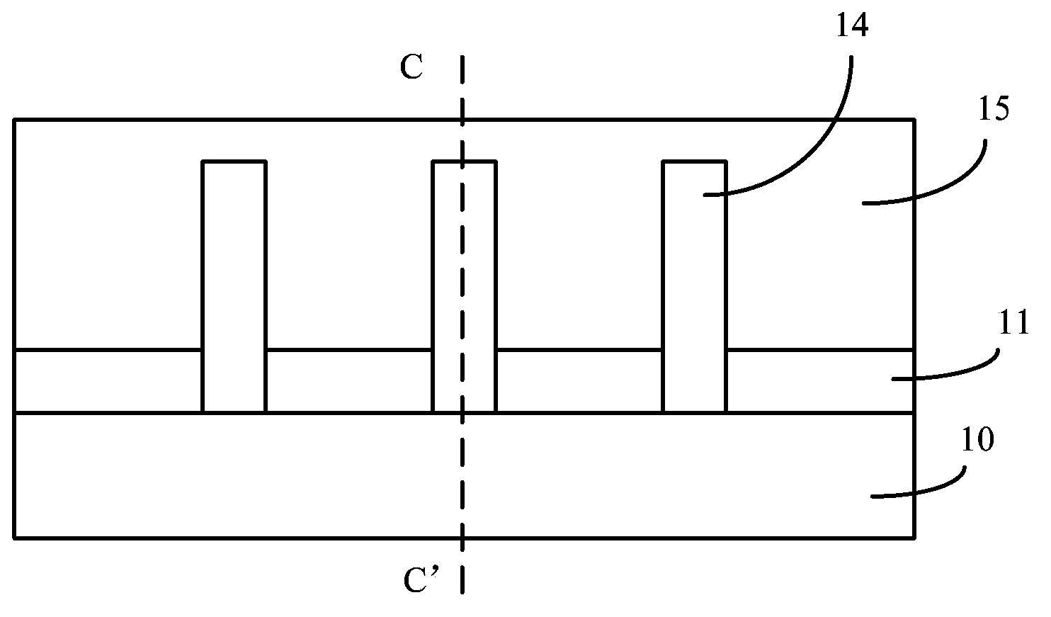
[0039] Please refer to Figure 4 , Figure 4 based on image ...


PUM

PropertyMeasurementUnit
Thicknessaaaaaaaaaa

Abstract

A method for forming a semiconductor structure comprises the steps of providing a substrate with the surface provided with a fin part; forming a first pseudo gate layer on the substrate and the surface of the pin part, enabling the surface of the first pseudo gate layer to be higher than the top surface of the fin part; flattening the first pseudo gate layer until the top surface of the fin part is exposed; after a flattening process, forming a second pseudo gate layer on the first pseudo gate layer and the surface of the fin part; etching part of the first pseudo gate layer and the second pseudo gate layer until the top and the side wall surface of the fin part are exposed, and forming a pseudo gate striding over a side wall and the top surface of the fin part. In the formed semiconductor structure, uniformity and accuracy of the thickness of the gate structure on the top surface of the fin part are improved.

Description

technical field [0001] The invention relates to the technical field of semiconductor manufacturing, in particular to a method for forming a semiconductor structure. Background technique [0002] With the rapid development of semiconductor manufacturing technology, semiconductor devices are developing towards higher element density and higher integration. As the most basic semiconductor device, transistors are currently being widely used. Therefore, with the increase of component density and integration of semiconductor devices, the gate size of planar transistors is getting shorter and shorter. The ability of traditional planar transistors to control channel current Weakened, resulting in short channel effect, resulting in leakage current, and ultimately affecting the electrical performance of semiconductor devices. [0003] In order to overcome the short channel effect of the transistor and suppress the leakage current, the prior art proposes a fin field effect transistor ...

Claims


Application Information

Patent Timeline
IPC IPC(8): H01L21/336H01L21/28
CPCH01L29/42356H01L29/66795
Inventor 洪中山
Owner SEMICON MFG INT (SHANGHAI) CORP
Why Eureka
Try Eureka