Forming method of electric conduction structure

A technology of conductive structure and conductive layer, applied in the manufacturing of circuits, electrical components, semiconductor/solid-state devices, etc., can solve the problems of affecting device performance, poor quality of conductive plugs, etc., to ensure conductive performance, good morphology, and increased width. The effect of size

Active Publication Date: 2014-10-29
SEMICON MFG INT (SHANGHAI) CORP
View PDF7 Cites 16 Cited by
  • Summary
  • Abstract
  • Description
  • Claims
  • Application Information

AI Technical Summary

Problems solved by technology

[0008] However, as the feature size of the device is continuously reduced, the width of the conductive plug is also reduced accordingly, and voids (Void) are easily generated in the formed conductive plug, and the quality of the formed conductive plug is poor, which is likely to affect the performance of the device.

Method used


Image

  • Forming method of electric conduction structure
  • Forming method of electric conduction structure
  • Forming method of electric conduction structure

Examples


Embodiment Construction

[0035] As mentioned in the background art, voids are easily generated in the conductive plug formed in the prior art, and its quality is poor and its performance is unstable.

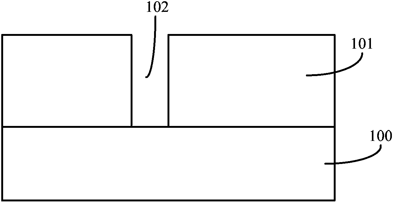
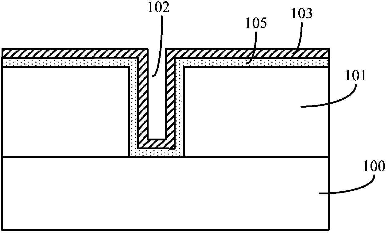
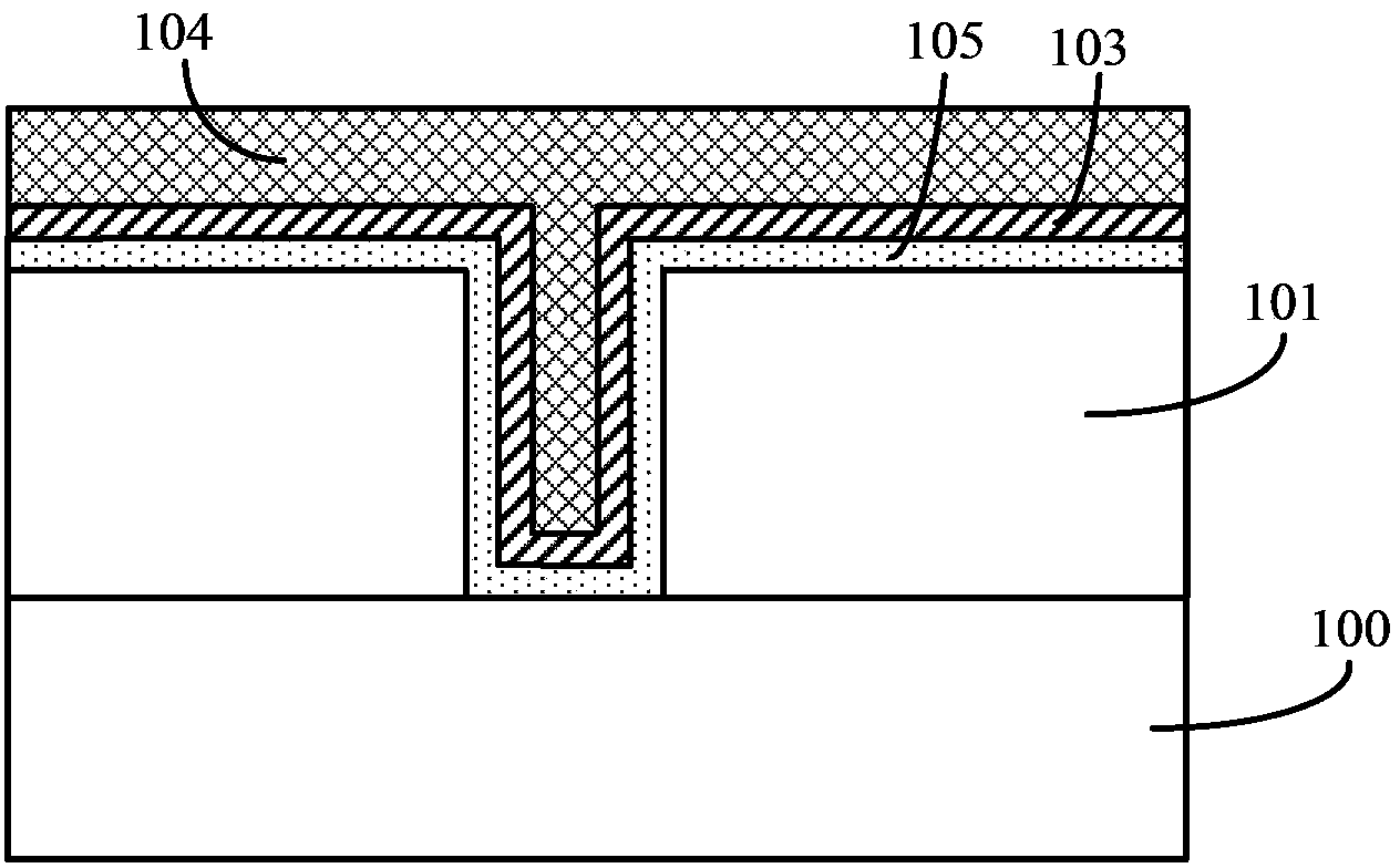
[0036] After research by the inventor of the present invention, please continue to refer to Figure 1 to Figure 4 , as the feature size of the device is continuously reduced, the width of the top of the opening 102 is also continuously reduced, resulting in an increase in the aspect ratio (Aspect Ratio) of the opening 102. Currently, the aspect ratio of the opening used to form a conductive plug is greater than 5: 1. The seed layer 103 is formed on the sidewall and bottom surface of the opening 102 by atomic layer deposition or physical vapor deposition. However, as the aspect ratio of the opening 102 increases and the width of the top of the opening 102 shrinks, the seed layer More material is accumulated on the sidewall surface near the top of the opening 102; after the seed layer is formed, the width...


PUM

PropertyMeasurementUnit
widthaaaaaaaaaa
thicknessaaaaaaaaaa

Abstract

A forming method of an electric conduction structure comprises providing a substrate, wherein the surface of the substrate is provided with a dielectric layer and the dielectric layer is provided with an opening; forming seed layers on surfaces of the lateral wall and the bottom of the opening; implanting modified ions into partial seed layer on the lateral wall surface which is close to the top of the opening through the iron implantation technology; utilizing the thermal annealing technology after the iron implantation technology to enable the partial seed layer with the modified irons being implanted to form into a sacrificial layer, wherein materials of the sacrificial layer and the seed layer are different; removing the sacrificial layer; forming an electric conducting layer in the opening after the sacrificial layer is removed, wherein the opening is full of the electric conducting layer. The formed electric conducting layer is free of gaps internally and good in quality.

Description

technical field [0001] The invention relates to the technical field of semiconductor manufacturing, in particular to a method for forming a conductive structure. Background technique [0002] In the integrated circuit manufacturing process, conductive plugs are often used for electrical interconnection between devices. With the rapid development of integrated circuit manufacturing technology, the size of semiconductor devices is continuously reduced, and the process of forming conductive plugs is also challenged. [0003] The schematic diagram of the cross-sectional structure of the process of forming the conductive plug in the prior art is as follows: Figure 1 to Figure 4 shown. [0004] Please refer to figure 1 , the substrate 100 has a dielectric layer 101 on its surface, and the dielectric layer 101 has an opening 102 therein for forming a conductive plug. [0005] Please refer to figure 2 , depositing a barrier layer 105 and a seed layer 103 on the surface of the...

Claims


Application Information

Patent Timeline
Patent Type & Authority Applications(China)
IPC IPC(8): H01L21/768
CPCH01L21/76865H01L21/76897
Inventor 邓浩周鸣洪中山
Owner SEMICON MFG INT (SHANGHAI) CORP
Why Eureka
Try Eureka