Bipolar thin film transistor and preparation method thereof
A thin film transistor and bipolar technology, applied in the field of bipolar thin film transistor and its preparation, can solve the problems of poor bipolarity of bipolar thin film transistors, achieve the effect of improving symmetry and solving poor symmetry
- Summary
- Abstract
- Description
- Claims
- Application Information
AI Technical Summary
Problems solved by technology
Method used
Image

Examples
preparation example Construction
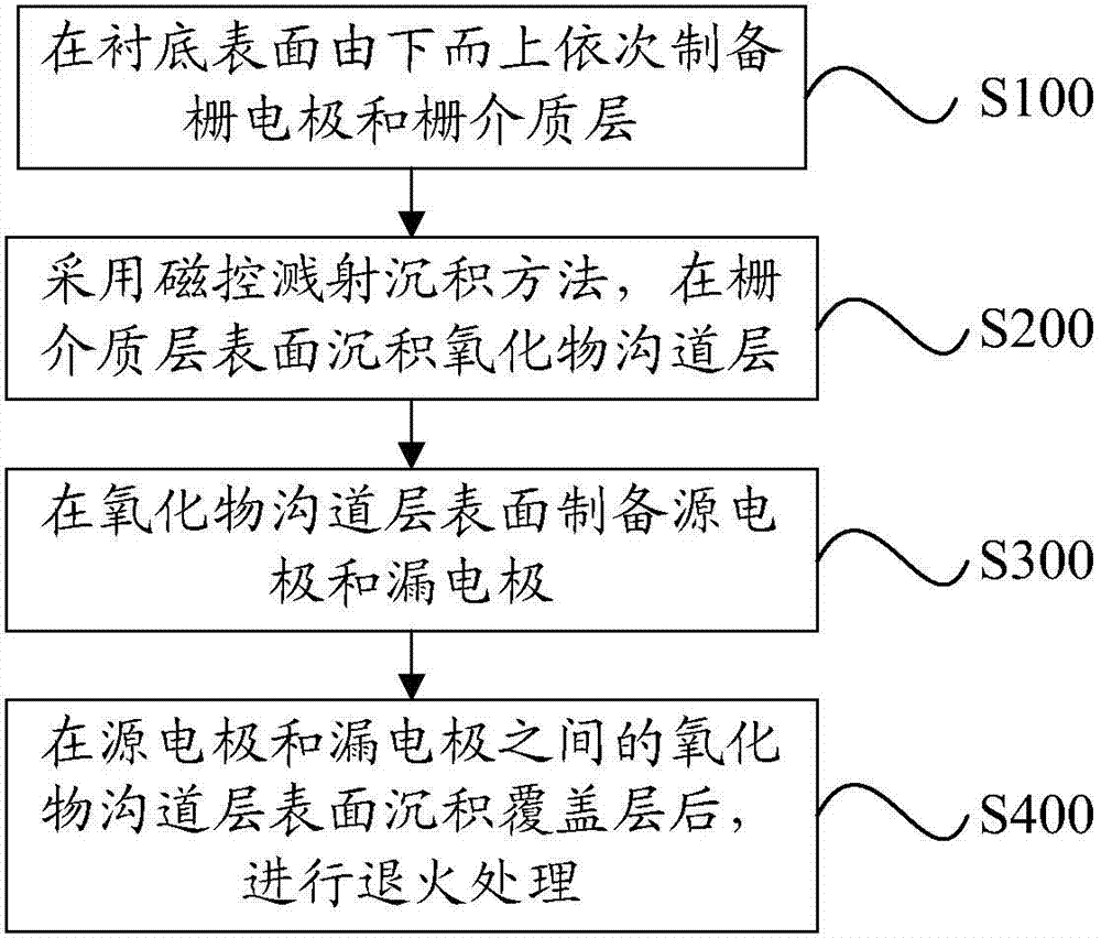
[0062] see image 3 , as a specific embodiment of the bipolar thin film transistor preparation method, comprising the following steps:
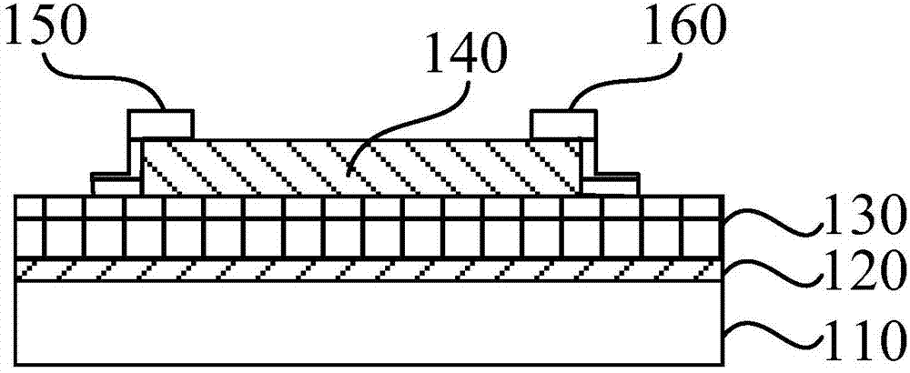
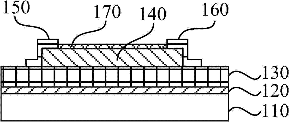
[0063] In step S100, a gate electrode and a gate dielectric layer are sequentially prepared on the surface of the substrate from bottom to top.
[0064] In step S200, a magnetron sputtering deposition method is used to deposit an oxide channel layer on the surface of the gate dielectric layer.
[0065] In step S300, a source electrode and a drain electrode are prepared on the surface of the oxide channel layer.
[0066] Step S400, after depositing a capping layer on the surface of the oxide channel layer between the source electrode and the drain electrode, perform annealing treatment.
[0067] Among them, the negative charge in the capping layer is used to adjust the hole concentration in the oxide channel layer.
[0068] By adopting the preparation method of the bipolar thin film transistor provided by the present invention, after the ga...
Embodiment 1
[0081] A method for preparing a bipolar thin film transistor according to a specific embodiment of the present invention includes the following steps:
[0082] Step S110, select an n-type heavily doped thermally oxidized silicon wafer with a crystal orientation of 100, n + -Si / SiO 2 (100) is used as a substrate, and is cleaned and dried. Among them, an n-type heavily doped thermally oxidized silicon wafer is selected as the substrate. The n-type heavily doped thermally oxidized silicon wafer can be used as a substrate, a gate electrode and a gate dielectric layer at the same time, eliminating the need to prepare a gate electrode and a gate dielectric. layer steps, saving process time and process resources. In addition, by cleaning and drying the n-type heavily doped thermally oxidized silicon wafer, the cleanliness of the substrate is ensured, and the phenomenon of contaminating the oxide channel layer prepared subsequently is avoided.
[0083] Among them, the gate dielectr...
Embodiment 5
[0113] The preparation method of the bipolar thin film transistor of the present invention comprises the following steps:
[0114] Step S120, selecting an n-type heavily doped thermally oxidized silicon wafer with 100 crystal orientation, n + -Si / SiO 2 (100) is used as a substrate, and is cleaned and dried. This step is the same as step S110 in Embodiment 1.
[0115] Step S220, using the magnetron sputtering deposition method, at n + -Si / SiO 2 (100) A tin oxide film is deposited on the surface as an oxide channel layer. Wherein, when the magnetron sputtering equipment is used for sputtering deposition of the tin oxide thin film, the target material used is a metal tin target. The working gas is a mixed gas of argon and oxygen, and the content of oxygen is 11.8%. The sputtering power was 40W and the gas pressure was 0.24Pa. The deposition temperature was room temperature. The thickness of the final prepared stannous oxide film is 24 nm, and the length and width are 100 ...
PUM
 Abstract
Description
Claims
Application Information
 - R&D
- Intellectual Property
- Life Sciences
- Materials
- Tech Scout
- Unparalleled Data Quality
- Higher Quality Content
- 60% Fewer Hallucinations
Browse by: Latest US Patents, China's latest patents, Technical Efficacy Thesaurus, Application Domain, Technology Topic, Popular Technical Reports.
© 2025 PatSnap. All rights reserved.Legal|Privacy policy|Modern Slavery Act Transparency Statement|Sitemap|About US| Contact US: help@patsnap.com