On-chip integrated optical digital-to-analog converter based on silicon-based nanowire waveguide

A digital-to-analog converter, silicon-based nanotechnology, used in optical analog/digital converters, optics, instruments, etc., can solve the problems of long waveguides, contradicting miniaturization goals, and difficult to accurately control the length of optical fibers and optical phases. The conversion number has the effect of realizing integration and miniaturization, and the scalability of the conversion number

Inactive Publication Date: 2014-11-05
INST OF SEMICONDUCTORS - CHINESE ACAD OF SCI
View PDF2 Cites 24 Cited by
  • Summary
  • Abstract
  • Description
  • Claims
  • Application Information

AI Technical Summary

Problems solved by technology

[0007] The document "All-optical digital-to-analog conversion using nonlinear optical loop mirrors" (IEEE Photonics Technology Letters, Vol.18, Iss.5, 2006, pp.703-705) uses a fiber optic loop mirror to achieve a resolution of 2bit, An all-optical integrated digital-to-analog converter with a conversion rate of 1MHz. Because the length of the optical fiber and the optical phase are difficult to control precisely, this technology has limitations in conversion accuracy and scalability
The document "Integrated optical digital-to-analogue converter and its application to pulse pattern recognition" (Electronics Letters, Vol.37, Iss.20, 2001, pp.1237-1238) reported the integrated digital-to-analogue converter based on silicon-based optical waveguide delay line Mode conversion structure, but to achieve a high-resolution DAC must use a longer waveguide, contrary to the miniaturization goal
In addition, since the phase difference of the optical signal after transmission between the waveguides is fixed, the device can only work at a fixed sampling rate

Method used


Image

  • On-chip integrated optical digital-to-analog converter based on silicon-based nanowire waveguide
  • On-chip integrated optical digital-to-analog converter based on silicon-based nanowire waveguide
  • On-chip integrated optical digital-to-analog converter based on silicon-based nanowire waveguide

Examples


Embodiment Construction

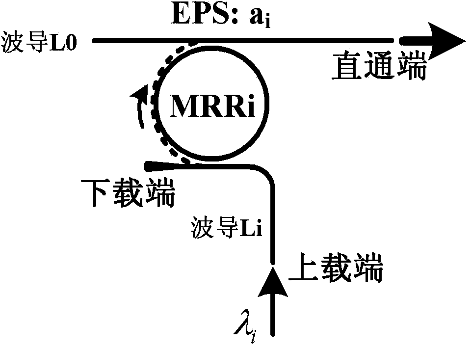
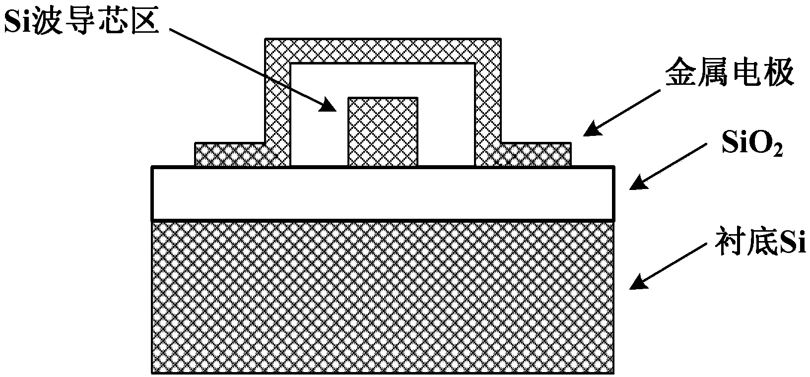
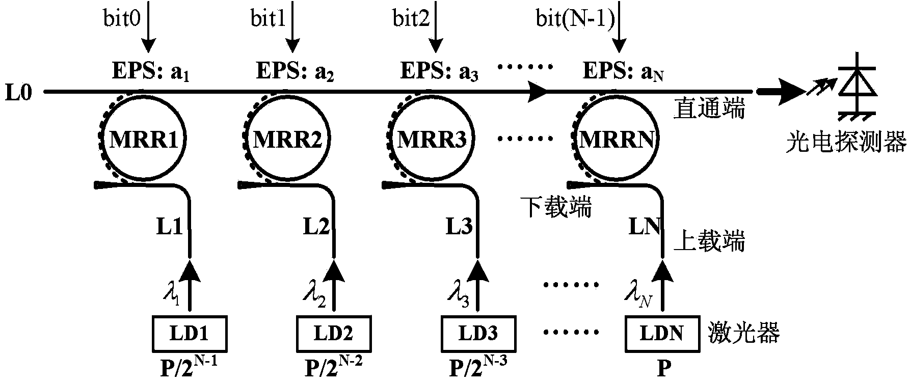
[0026] In order to make the object, technical solution and advantages of the present invention clearer, the present invention will be described in further detail below in conjunction with specific embodiments and with reference to the accompanying drawings.

[0027] It should be noted that, in the drawings or descriptions of the specification, similar or identical parts all use the same figure numbers. Implementations not shown or described in the accompanying drawings are forms known to those of ordinary skill in the art. Additionally, while illustrations of parameters including particular values ​​may be provided herein, it should be understood that the parameters need not be exactly equal to the corresponding values, but rather may approximate the corresponding values ​​within acceptable error margins or design constraints. In addition, the directional terms mentioned in the following embodiments, such as "upper", "lower", "front", "rear", "left", "right", etc., are only re...


PUM

PropertyMeasurementUnit
refractive indexaaaaaaaaaa

Abstract

The invention discloses an on-chip integrated optical digital-to-analog converter based on a silicon-based nanowire waveguide. The on-chip integrated optical digital-to-analog converter comprises N laser devices, a modulation multiplex integral structure and a photoelectric detector. The modulation multiplex integral structure comprises a trunk waveguide L0, N cascaded silicon-based nanowire waveguide micro-ring resonators (MRR1, MRR2...MRRN) and N bent waveguides (L1, L2...LN), the N laser devices are connected with the uploading ends of the N bent waveguides (L1, L2...LN) respectively, the photoelectric detector is connected with the straight-through end of the trunk waveguide L0, and N is a natural number. According to the on-chip integrated optical digital-to-analog converter, the advantages that the silicon-based waveguide is compact in structure, low in power consumption, compatible with the CMOS process and the like are fully achieved, the high speed and high resolution in the DAC process can be achieved, and the integration and miniaturization of the optical DAC can be achieved.

Description

technical field [0001] The invention belongs to the technical field of optical information processing and high-bandwidth signal processing, and in particular relates to an on-chip integrated optical digital-to-analog converter based on a silicon-based nanowire waveguide. Background technique [0002] In recent years, with the continuous improvement of information-based living standards, the information interaction and integration between the actual physical world that people exist and the virtual world of digital information processing is developing in the direction of diversification, refinement and high speed. Ultra-high-speed, high-resolution analog-to-digital converter (Analog-to-digital Converter, ADC) and digital-to-analog converter (Digital-to-analog Converter, DAC) as a bridge between the analog world and the digital world, in wireless communication , Biomedical, industrial automation, radar and sonar systems, aerospace, satellite communications and other high-bandwi...

Claims


Application Information

Patent Timeline
Patent Type & Authority Applications(China)
IPC IPC(8): G02F7/00
Inventor 周平杨林丁建峰张凡凡
Owner INST OF SEMICONDUCTORS - CHINESE ACAD OF SCI
Why Eureka
Try Eureka