USB (Universal Serial Bus) interface circuit

A USB interface and circuit technology, applied in the field of USB interface, can solve the problems of inductance L1 losing its protection function, grounding line without isolation design, USB signal easy to be distorted, etc.

Active Publication Date: 2014-11-05
蚌埠市野山坡网络科技有限公司
View PDF4 Cites 31 Cited by
  • Summary
  • Abstract
  • Description
  • Claims
  • Application Information

AI Technical Summary

Problems solved by technology

However figure 1 In the circuit shown, on the one hand, the grounding line is not designed for isolation, which leads to the direct conduction between the working ground GND and the output ground. As long as there is high voltage outside, it will directly enter the internal circuit of the device, causing damage to the machine. The insulation spacing is not enough to meet the requirements of the industry, and the withstand voltage cannot meet the requirements; on the other hand, the action time of diodes D1, D2, and D3 is ps level, while the action time of induct

Method used


Image

  • USB (Universal Serial Bus) interface circuit
  • USB (Universal Serial Bus) interface circuit
  • USB (Universal Serial Bus) interface circuit

Examples


Embodiment 1

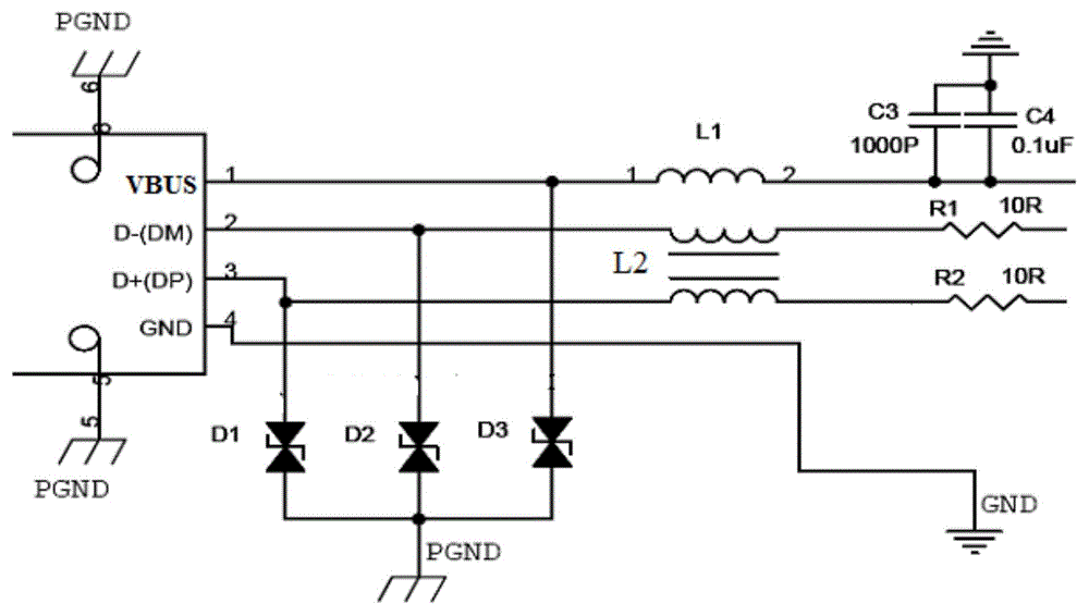
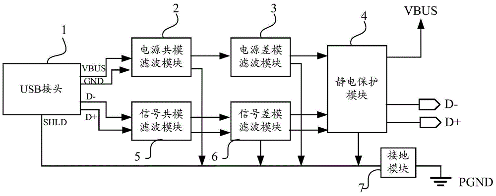
[0034] Please refer to figure 2 , this embodiment provides a USB interface circuit, including: a USB connector 1, a power supply common-mode filter module 2, a signal common-mode filter module 5, a power supply differential-mode filter module 3, a signal differential-mode filter module 6, and an electrostatic protection module 4 and Grounding module 7; wherein, the input end of the power supply common mode filtering module 2 is connected to the power terminal VBUS and the working ground terminal GND of the USB connector, for filtering common mode interference signals on the power line and the working ground line; The power supply differential mode filter module 3 is connected to the output end of the power supply common mode filter module 2 for filtering out differential mode interference signals on the power line; the input end of the signal common mode filter module 5 is connected to the USB connector The two terminals D- and D+ of the differential signal line are used to f...

Embodiment 2

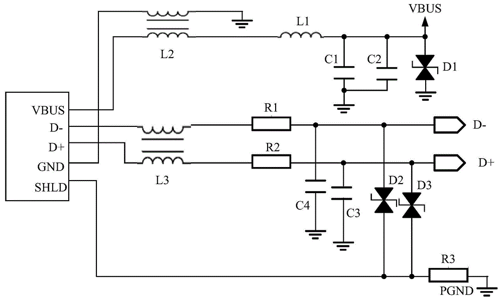
[0041] Please refer to Figure 4 , this embodiment provides a USB interface circuit, including: a USB connector 1, a power supply common-mode filter module 2, a signal common-mode filter module 5, a power supply differential-mode filter module 3, a signal differential-mode filter module 6, and an electrostatic protection module 4, Grounding module 7 and high voltage protection module 8 .

[0042] The difference between this embodiment and Embodiment 1 is that a high-voltage protection module 8 is added. One end of the high-voltage protection module 8 is connected to the shielding ground of the USB connector, and the other end is connected to the working ground line, the power line and the differential signal line. The protection module 8 can be set between the common-mode filter and the differential film filter, or before the common-mode filter or after the differential film filter, preferably before the differential film filter, to eliminate the working ground line, power lin...

Embodiment 3

[0047] Please refer to Figure 6 , this embodiment provides a USB interface circuit, including: a USB connector 1, a power supply common-mode filter module 2, a signal common-mode filter module 5, a power supply differential-mode filter module 3, a signal differential-mode filter module 6, and an electrostatic protection module 4, Grounding module 7 , high voltage protection module 8 and high frequency filter module 9 .

[0048] The difference between this embodiment and Embodiment 2 is that a high-frequency filter module 9 is added, and the high-frequency filter module 9 is set between the USB connector 1, the power supply common-mode filter module 2, and the signal common-mode filter module 5 to filter out the power supply High-frequency signal interference on line and differential signal lines.

[0049] In this embodiment, the high-frequency filter module 9 includes two filter inductors (or magnetic beads) L4, L5 and Two filter inductors (or magnetic beads) L6, L7 are res...


PUM


Abstract

The invention provides a USB (Universal Serial Bus) interface circuit which comprises a USB connector, a power common mode filter module, a signal common mode filter module, a power differential mode filter module, a signal differential mode filter module and an electrostatic protection module. Common mode interference, differential mode interference, electrostatic interference and the like on a power line and a signal line in the circuit can be eliminated; particularly, the additionally arranged power common mode filter module can eliminate common mode interference between a power VBUS and a working ground GND; and the circuit is small in size, low in cost and high in practicability, has very good protection effects on electrostatic discharge (ESD) and electromagnetic interference (EMI), allows a USB signal to be free from distortion, and ensures that a product smoothly passes USB certification and EMC (Electromagnetic Compatibility) certification. In addition, a high-voltage protection module and a high-frequency filter module can eliminate high-voltage signal interference and high-frequency signal interference in the circuit, so that the interference resistance of the USB interface circuit is further improved, and the signal transmission performance of the USB interface circuit is improved.

Description

technical field [0001] The invention relates to the technical field of USB interface, in particular to a USB interface circuit. Background technique [0002] Due to the development of multimedia technology, there is a higher demand for the data transmission rate between the peripheral and the host computer, so the USB bus technology emerges as the times require. USB (Universal Serial Bus) is translated into Chinese as Universal Serial Bus, which is jointly researched and developed by companies such as Conpaq, DEC, IBM, Inter, Microsoft, NEC and Northen Telecom to simplify the interconnection between PCs and peripherals. A free standardized connector, which is characterized by fast speed, good compatibility, no interruption, can be connected in series, supports hot plugging, etc. It supports various PCs and scanners, digital cameras, digital cameras, audio systems, monitors, The connection between peripherals such as input devices can also realize digital multimedia integrat...

Claims


Application Information

Patent Timeline
IPC IPC(8): H02M1/44H02M1/14
Inventor 林振翠
Owner 蚌埠市野山坡网络科技有限公司
Why Eureka
Try Eureka