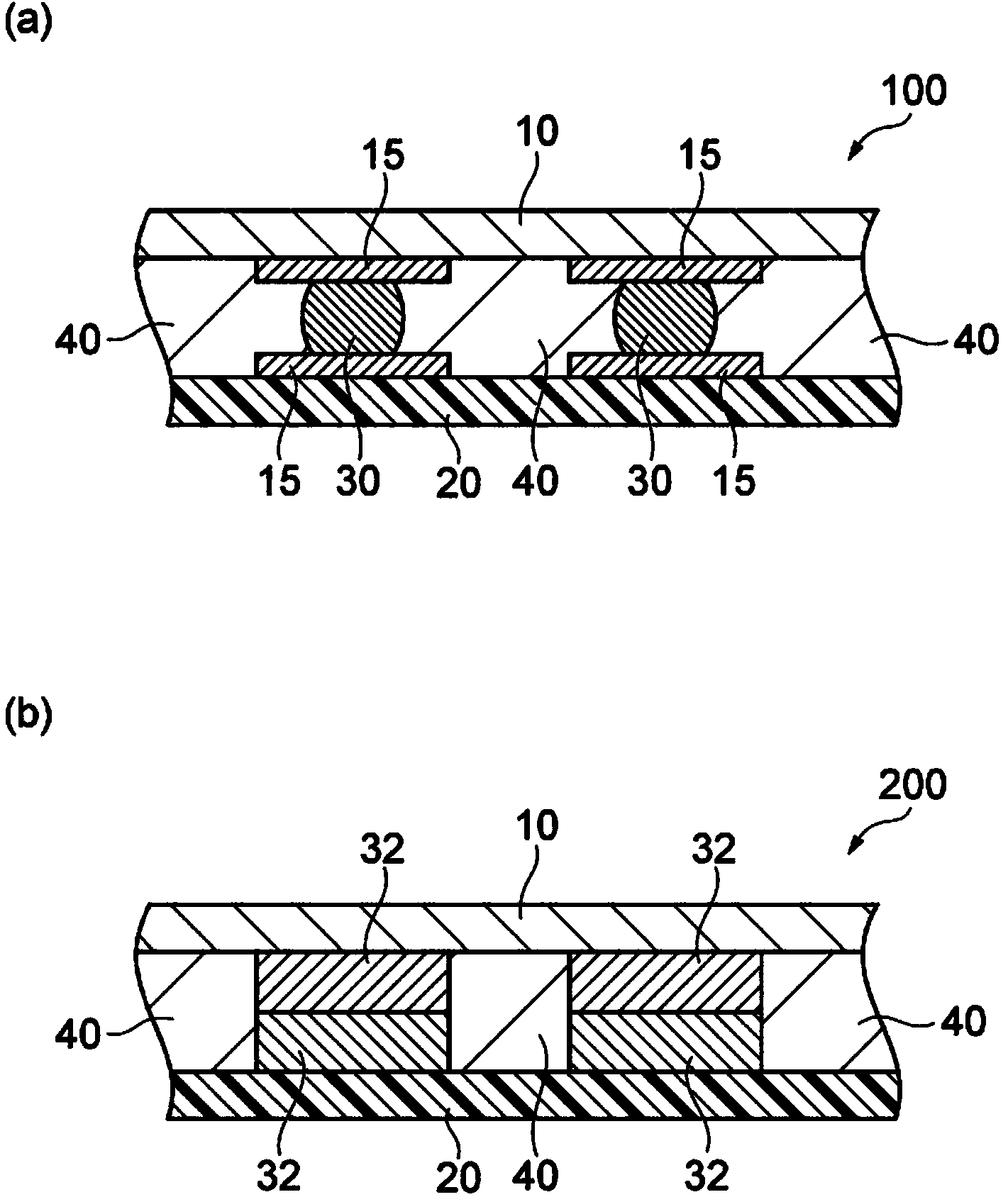
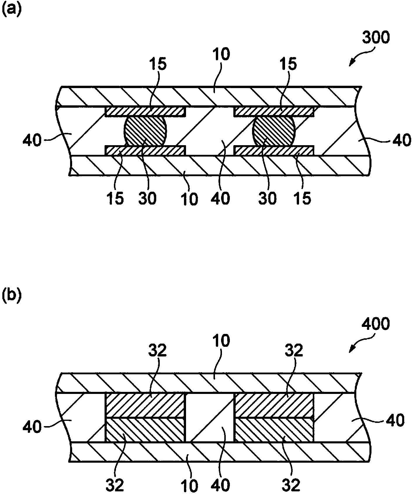
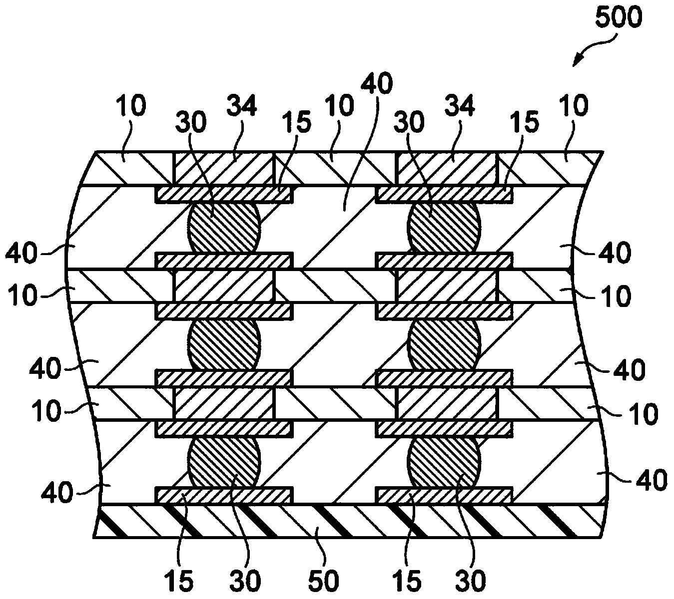
Adhesive for semiconductor, fluxing agent, manufacturing method for semiconductor device, and semiconductor device
A manufacturing method and semiconductor technology, applied in the fields of semiconductor/solid-state device manufacturing, semiconductor devices, non-polymer adhesive additives, etc., can solve the problem of reduced connectivity/insulation reliability, decreased connectivity, decreased solder wettability, etc. problem, to achieve the effect of excellent connection reliability and excellent reflow resistance
- Summary
- Abstract
- Description
- Claims
- Application Information
AI Technical Summary
Problems solved by technology
Method used
Image
Examples
Embodiment 1
[0238] Add 3g of epoxy resin ("EP1032" 2.4g, "YL983" 0.45g, "YL7175" 0.15g), curing agent "2MAOK" 0.1g, 2-methylglutaric acid 0.1g (0.69mmol), inorganic filler 1.9 g ("SE2050" 0.38g, "SE2050-SEJ" 0.38g, "SM nano silica" 1.14g), resin filler (EXL-2655) 0.25g and methyl ethyl ketone (amount to achieve 63% by mass of solid content), Beads having a diameter of 0.8 mm and beads having a diameter of 2.0 mm equal in weight to the solid content were added, and stirred for 30 minutes using a bead mill (Fritsch Japan Co., Ltd., planetary pulverizer P-7). Thereafter, 1.7 g of a phenoxy resin (ZX1356) was added and stirred again with a bead mill for 30 minutes, and then the beads used for stirring were removed by filtration to obtain a resin varnish.
[0239] The obtained resin varnish was coated on a substrate film (manufactured by Teijin DuPont Film Co., Ltd., trade name "Purex A53") with a small precision coating device (Yaijing Seiki), and dried in a clean oven (manufactured by ESPEC)...
Embodiment 2
[0240] (Example 2, Comparative Examples 1-6)
[0241] The film adhesive of Example 2 and the film adhesive of Comparative Examples 1-6 were produced similarly to Example 1 except having changed the composition of the material used as shown in following Table 1.
[0242] The evaluation methods of the film adhesives obtained in Examples and Comparative Examples are shown below.
[0243]
[0244] Cut the film-like adhesive produced in the embodiment or comparative example into a prescribed size (8mm in length x 8mm in width x 0.045mm in thickness), and paste it on a glass epoxy substrate (glass epoxy substrate: 420 μm thick, Copper wiring: 9μm thick), a semiconductor chip with solder bumps (chip size: 7.3mm in length x 7.3mm in width x 0.15mm in thickness, bump height: about 40μm in copper pillar + solder, 328 bumps) Mounting was performed using a flip mounting device "FCB3" (trade name, manufactured by Panasonic) (mounting conditions: crimping head temperature: 350° C., crimpin...
PUM
| Property | Measurement | Unit |
|---|---|---|
| melting point | aaaaa | aaaaa |
| melting point | aaaaa | aaaaa |
| height | aaaaa | aaaaa |
Abstract
Description
Claims
Application Information
 - R&D
- Intellectual Property
- Life Sciences
- Materials
- Tech Scout
- Unparalleled Data Quality
- Higher Quality Content
- 60% Fewer Hallucinations
Browse by: Latest US Patents, China's latest patents, Technical Efficacy Thesaurus, Application Domain, Technology Topic, Popular Technical Reports.
© 2025 PatSnap. All rights reserved.Legal|Privacy policy|Modern Slavery Act Transparency Statement|Sitemap|About US| Contact US: help@patsnap.com


