
CCD device quantum efficiency measuring device and method

A quantum efficiency and measurement device technology, which is applied in the direction of testing optical performance, etc., can solve the problems of large loss of light energy, reduced accuracy of quantum efficiency of CCD devices, and inability to meet high-quality testing requirements, etc.

Active Publication Date: 2014-11-12
THE 41ST INST OF CHINA ELECTRONICS TECH GRP
View PDF7 Cites 13 Cited by
  • Summary
  • Abstract
  • Description
  • Claims
  • Application Information

AI Technical Summary

Problems solved by technology

[0006] Among the above methods, the absolute quantum efficiency of the CCD device is measured. First, the quantum efficiency of a certain wavelength point is obtained through a narrow linewidth filter, and then the absolute quantum efficiency of the entire response band is calculated by measuring the relative spectral response of the CCD device. This method The disadvantage of the method of obtaining the quantum efficiency of CCD devices is that when obtaining the absolute quantum efficiency of a certain wavelength point, a filter with a narrow linewidth is used to achieve it. From the current research situation, the linewidth of a good filter with a narrow linewidth is generally It is about 10nm, and the light passing filter is generally about 60%, and the loss of light energy is relatively large.
As a result, the accuracy of the measured quantum efficiency of the CCD device is reduced, which cannot meet the requirements of high-quality testing

Method used


Image

  • CCD device quantum efficiency measuring device and method
  • CCD device quantum efficiency measuring device and method
  • CCD device quantum efficiency measuring device and method

Examples


Embodiment 1

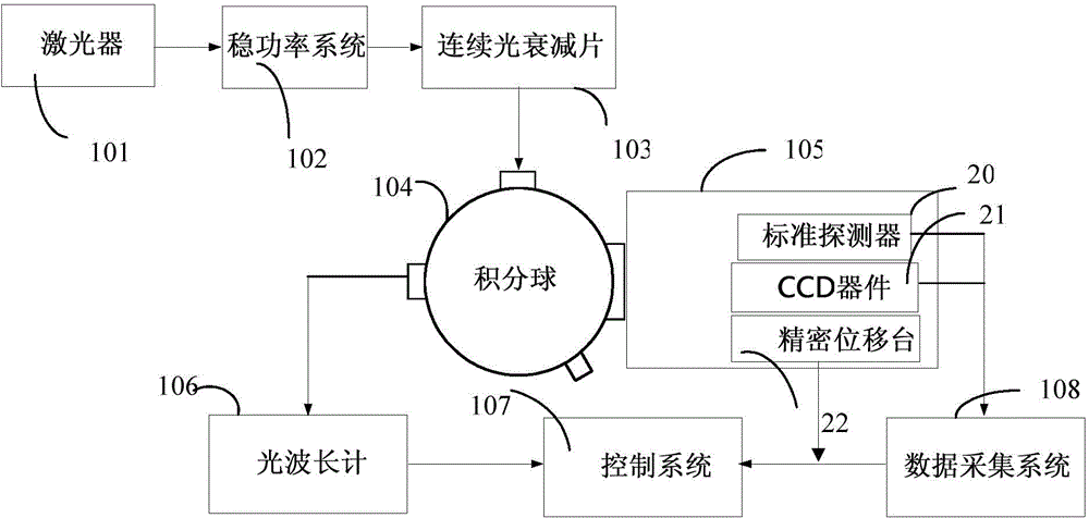
[0045] Such as figure 1 As shown, a CCD device absolute quantum efficiency measuring device is used to measure the absolute quantum efficiency of the CCD device at the 632.8nm wavelength point; the CCD device absolute quantum efficiency measuring device consists of a laser 101, a power stabilization system 102, and a continuous light attenuation sheet 103 (it can also be a continuously adjustable light attenuating film) is connected in sequence with the integrating sphere 104, the laser 101 is used to output light with a wavelength of 632.8nm; the power stabilization system 102 is used to stabilize the light , the continuous light attenuating sheet 103 is used to attenuate the light so that the light received by the CCD device 21 is within the linear range of the integrating sphere 104; the integrating sphere 104 is also provided with the optical wavelength meter 106 and the shielding room 105 to be connected respectively, The optical wavelength meter 106 is used to measure th...

Embodiment 2

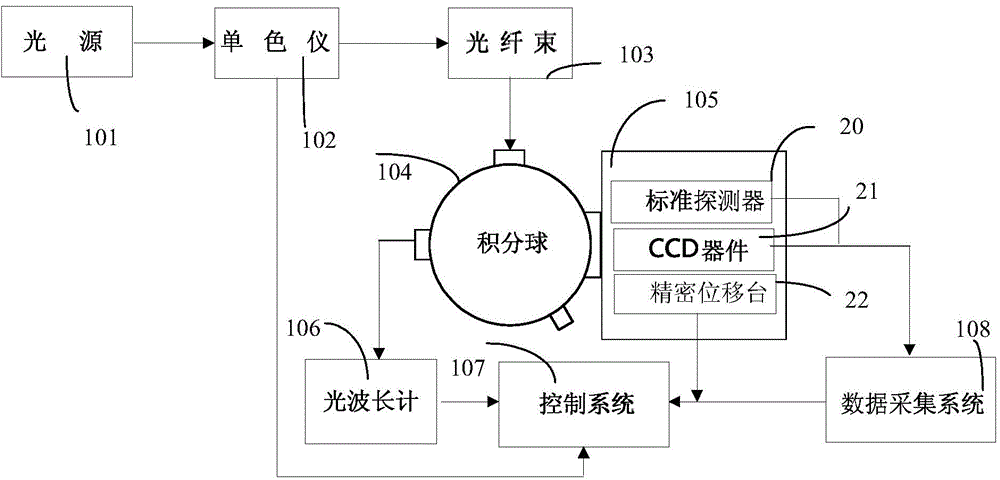
[0057] Such as figure 2Shown, in the present invention, the CCD device relative quantum efficiency measuring device is connected with the integrating sphere 104 after being sequentially connected by a light source 101, a monochromator 102, and an optical fiber bundle 103, and the described light source 101 adopts a xenon lamp as a light source for generating wide Spectral light source; the monochromator 102 is used to split the wide-spectrum light source input to the monochromator 102 to generate monochromatic light; the optical focusing system is used to converge the monochromatic light output by the monochromator 102, The light is converged into the fiber bundle 103; the integrating sphere 104 is connected with the optical wavelength meter 106 and the shielding room 105 respectively, and the optical wavelength meter 106 is used to measure the wavelength output by the integrating sphere 104; the shielding room 105 uses To shield stray light, to avoid the impact of stray ligh...

Embodiment 3

[0071] A method for measuring the quantum efficiency of a CCD device, which includes a method for measuring the absolute quantum efficiency of a CCD device for measuring the absolute quantum efficiency of a CCD device at a wavelength point of 632.8nm; and a method for measuring the relative quantum efficiency of a CCD device for measuring the CCD device at Relative quantum efficiency in the wavelength range of 300nm to 1100nm.

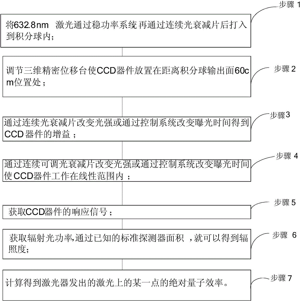
[0072] Further, if image 3 Shown, described CCD device quantum efficiency measurement method, wherein, described CCD device absolute quantum efficiency measurement method, comprises the following steps:

[0073] Step 1: Pass the 632.8nm laser through the power stabilization system, then pass through the continuous light attenuation film and inject it into the integrating sphere;

[0074] Step 2: Adjust the three-dimensional precision translation stage so that the CCD device is placed at a position 60cm away from the output surface of the integrating ...


PUM

PropertyMeasurementUnit
Diameteraaaaaaaaaa
Diameteraaaaaaaaaa

Abstract

The invention provides a CCD device quantum efficiency measuring device and method. The device comprises a CCD device absolute quantum efficiency measuring apparatus and a CCD device relative quantum efficiency measuring apparatus, the CCD device absolute quantum efficiency measuring apparatus is used for measuring the absolute quantum efficiency of a CCD device on a 632.8 nm wavelength point, and the CCD device relative quantum efficiency measuring apparatus is used for measuring the relative quantum efficiency of the CCD device within the wavelength range from 300 nm to 1100 nm. According to the CCD device quantum efficiency measuring device and method, a 632.8 nm laser is used for emitting light into an integrating sphere to carry out absolute calibration after the light passes through a power stabilizing system, lasers with different levels of output power can be selected according to different CCD devices, the problem that optical power is low is avoided, no light loss is caused, a standard detector directly traces the source to a low-temperature radiometer on the 632.8 nm wavelength point, and therefore the number of intermediate links is reduced, and uncertainty of measurement is improved.

Description

technical field [0001] The invention belongs to the technical field of quantum efficiency measurement, and in particular relates to a device and method for measuring the absolute quantum efficiency and relative quantum efficiency of a CCD device. Background technique [0002] At present in China, the quantum efficiency of a certain wavelength point is obtained through halogen lamps, integrating spheres, standard detectors, and narrow linewidth filters, and then the quantum efficiency of the entire response band is calculated by measuring the relative spectral response of the CCD device. This method obtains The disadvantage of the quantum efficiency method of CCD devices is that when obtaining the absolute quantum efficiency of a certain wavelength point, a filter with a narrow linewidth is used to achieve it. From the current research situation, the linewidth of a good filter with a narrow linewidth is generally between It is about 10nm, and the light passing filter is gener...

Claims


Application Information

Patent Timeline
IPC IPC(8): G01M11/02
Inventor 刘红元王恒飞王洪超应承平吴斌史学舜李国超
Owner THE 41ST INST OF CHINA ELECTRONICS TECH GRP
Learn More